Functional description – Rainbow Electronics АDC0805 User Manual
Page 16
Functional Description
(Continued)
The voltage on this capacitance is switched and will result in
currents entering the V
IN
(a) input pin and leaving the
V
IN
(b) input which will depend on the analog differential
input voltage levels These current transients occur at the
leading edge of the internal clocks They rapidly decay and
do not cause errors
as the on-chip comparator is strobed at
the end of the clock period
Fault Mode
If the voltage source applied to the V
IN
(a) or V
IN
(b) pin
exceeds the allowed operating range of V
CC
a
50 mV large
input currents can flow through a parasitic diode to the V
CC
pin If these currents can exceed the 1 mA max allowed
spec an external diode (1N914) should be added to bypass
this current to the V
CC
pin (with the current bypassed with
this diode the voltage at the V
IN
(a) pin can exceed the
V
CC
voltage by the forward voltage of this diode)
2 3 2 Input Bypass Capacitors
Bypass capacitors at the inputs will average these charges
and cause a DC current to flow through the output resist-
ances of the analog signal sources This charge pumping
action is worse for continuous conversions with the V
IN
(a)
input voltage at full-scale For continuous conversions with
a 640 kHz clock frequency with the V
IN
(a) input at 5V this
DC current is at a maximum of approximately 5 mA There-
fore
bypass capacitors should not be used at the analog
inputs or the V
REF
2 pin
for high resistance sources (
l
1
kX) If input bypass capacitors are necessary for noise filter-
ing and high source resistance is desirable to minimize ca-
pacitor size the detrimental effects of the voltage drop
across this input resistance which is due to the average
value of the input current can be eliminated with a full-scale
adjustment while the given source resistor and input bypass
capacitor are both in place This is possible because the
average value of the input current is a precise linear func-
tion of the differential input voltage
2 3 3 Input Source Resistance
Large values of source resistance where an input bypass
capacitor is not used
will not cause errors
as the input cur-
rents settle out prior to the comparison time If a low pass
filter is required in the system use a low valued series resis-
tor (
s
1 kX) for a passive RC section or add an op amp RC
active low pass filter For low source resistance applica-
tions (
s
1 kX) a 0 1 mF bypass capacitor at the inputs will
prevent noise pickup due to series lead inductance of a long
wire A 100X series resistor can be used to isolate this ca-
pacitor
both the R and C are placed outside the feedback
loop
from the output of an op amp if used
2 3 4 Noise
The leads to the analog inputs (pin 6 and 7) should be kept
as short as possible to minimize input noise coupling Both
noise and undesired digital clock coupling to these inputs
can cause system errors The source resistance for these
inputs should in general be kept below 5 kX Larger values
of source resistance can cause undesired system noise
pickup Input bypass capacitors placed from the analog in-
puts to ground will eliminate system noise pickup but can
create analog scale errors as these capacitors will average
the transient input switching currents of the A D (see sec-
tion 2 3 1 ) This scale error depends on both a large source
resistance and the use of an input bypass capacitor This
error can be eliminated by doing a full-scale adjustment of
the A D (adjust V
REF
2 for a proper full-scale reading
see
section 2 5 2 on Full-Scale Adjustment) with the source re-
sistance and input bypass capacitor in place
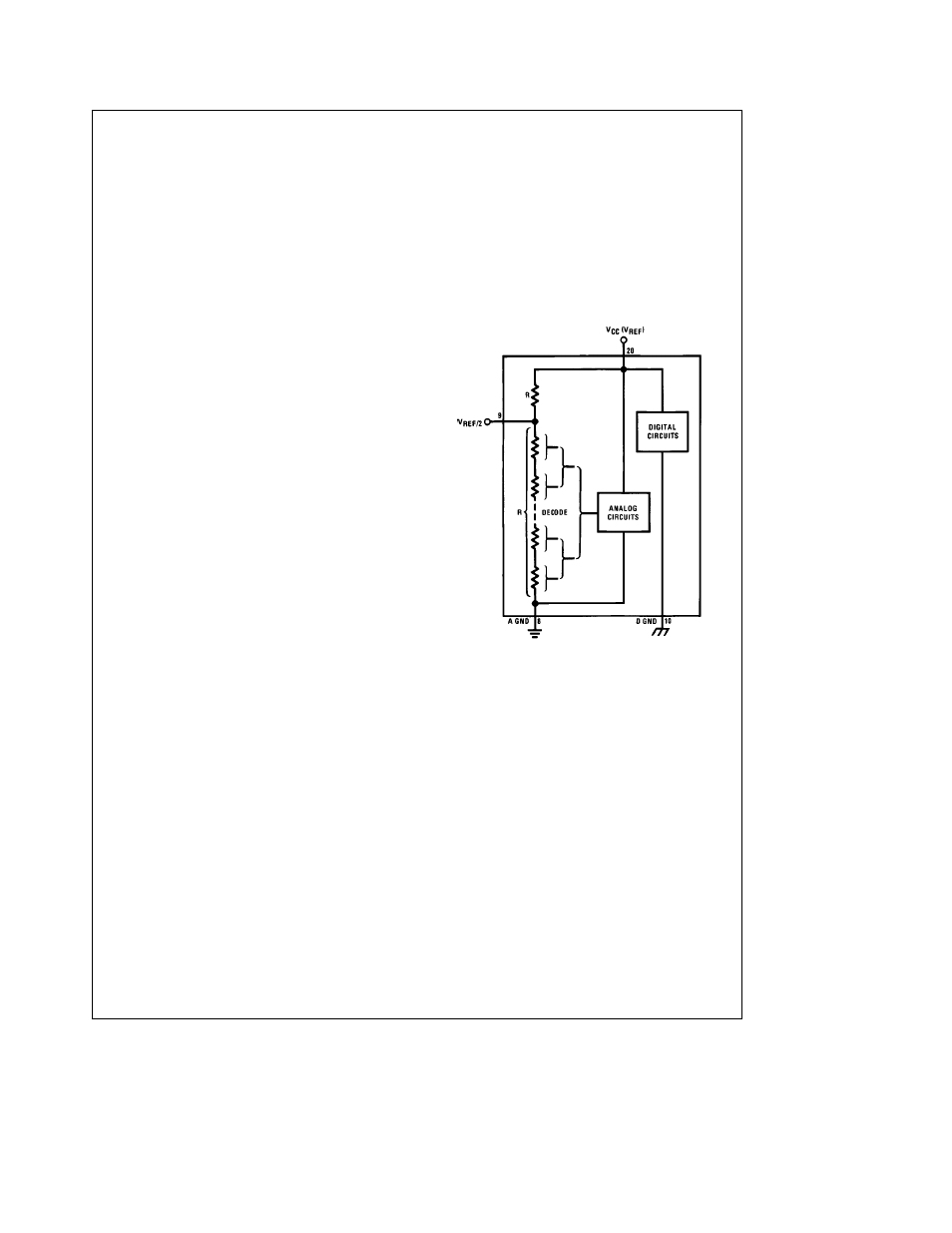
2 4 Reference Voltage
2 4 1 Span Adjust
For maximum applications flexibility these A Ds have been
designed to accommodate a 5 V
DC
2 5 V
DC
or an adjusted
voltage reference This has been achieved in the design of
the IC as shown in
Figure 4
TL H 5671 – 15
FIGURE 4 The V
REFERENCE
Design on the IC
Notice that the reference voltage for the IC is either
of
the voltage applied to the V
CC
supply pin or is equal to the
voltage that is externally forced at the V
REF
2 pin This al-
lows for a ratiometric voltage reference using the V
CC
sup-
ply a 5 V
DC
reference voltage can be used for the V
CC
supply or a voltage less than 2 5 V
DC
can be applied to the
V
REF
2 input for increased application flexibility The inter-
nal gain to the V
REF
2 input is 2 making the full-scale differ-
ential input voltage twice the voltage at pin 9
An example of the use of an adjusted reference voltage is to
accommodate a reduced span
or dynamic voltage range
of the analog input voltage If the analog input voltage were
to range from 0 5 V
DC
to 3 5 V
DC
instead of 0V to 5 V
DC
the span would be 3V as shown in
Figure 5
With 0 5 V
DC
applied to the V
IN
(b) pin to absorb the offset the reference
voltage can be made equal to
of the 3V span or 1 5 V
DC
The A D now will encode the V
IN
(a) signal from 0 5V to 3 5
V with the 0 5V input corresponding to zero and the 3 5 V
DC
input corresponding to full-scale The full 8 bits of resolution
are therefore applied over this reduced analog input voltage
range
16