Functional description – Rainbow Electronics АDC0805 User Manual
Page 21
Functional Description
(Continued)
TL H 5671 – 20
Note 1
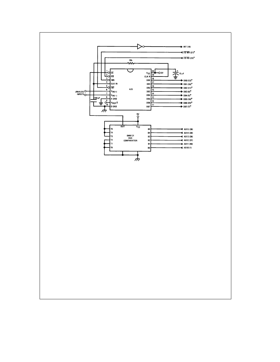
Pin numbers for the DP8228 system controller others are INS8080A
Note 2
Pin 23 of the INS8228 must be tied to
a
12V through a 1 kX resistor to generate the RST 7
instruction when an interrupt is acknowledged as required by the accompanying sample program
FIGURE 10 ADC0801 – INS8080A CPU Interface
SAMPLE PROGRAM FOR
FIGURE 10
ADC0801 – INS8080A CPU INTERFACE
0038
C3 00 03
RST 7
JMP
LD DATA
0100
21 00 02
START
LXI H 0200H
HL pair will point to
data storage locations
0103
31 00 04
RETURN
LXI SP 0400H
Initialize stack pointer (Note 1)
0106
7D
MOV A
L
Test
of bytes entered
0107
FE OF
CPI OF H
If
4 16 JMP to
0109
CA 13 01
JZ CONT
user program
010C
D3 E0
OUT E0 H
Start A D
010E
FB
EI
Enable interrupt
010F
00
LOOP
NOP
Loop until end of
0110
C3 OF 01
JMP LOOP
conversion
0113
CONT
(User program to
process data)
0300
DB E0
LD DATA
IN E0 H
Load data into accumulator
0302
77
MOV M
A
Store data
0303
23
INX H
Increment storage pointer
0304
C3 03 01
JMP RETURN
Note 1
The stack pointer must be dimensioned because a RST 7 instruction pushes the PC onto the stack
Note 2
All address used were arbitrarily chosen
21