Table 7. recommended timing adjustments (v, Table 9. reset methods – Rainbow Electronics MAX19515 User Manual
Page 30
MAX19515
Dual-Channel, 10-Bit, 65Msps ADC
30
______________________________________________________________________________________
Integrated Voltage Regulator
The MAX19515 includes an integrated self-sensing lin-
ear voltage regulator on the analog supply (AVDD). See
Figure 17. When the applied voltage on AVDD is below
2V, the voltage regulator is bypassed, and the core
analog circuitry operates from the externally applied
voltage. If the applied voltage on AVDD is higher than
2V, the regulator bypass switches off, and voltage reg-
ulator mode is enabled. When in voltage regulation
mode, the internal-core analog circuitry operates from a
stable 1.8V supply voltage provided by the regulator.
The regulator provides an output voltage of 1.8V over a
2.3V to 3.5V AVDD input-voltage range. Since the
power-supply current is constant over this voltage
range, analog power dissipation is proportional to the
applied voltage.
Power-On and Reset
The user-programmable register default settings and
other factory-programmed settings are stored in non-
volatile memory. Upon device power-up, these values are
loaded into the control registers. This operation occurs
after application of supply voltage to AVDD and applica-
tion of an input clock signal. The register values are
retained as long as AVDD is applied. While AVDD is
applied, the registers can be reset, which will overwrite all
user-programmed registers with the default values. This
reset operation can be initiated by software command
through the serial-port interface or by hardware control
using the SPEN and SHDN inputs. The reset time is pro-
portional to the ADC clock period and requires 130µs at
65Msps. Table 9 summarizes the reset methods.
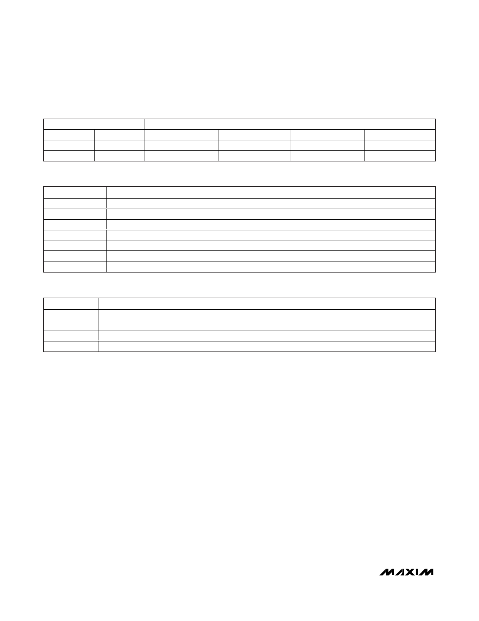
SAMPLING RATE (Msps)
V
OVDD
= 3.3V
FROM
TO
DA_BYPASS
DLY_HALF_T
DTIME<2:0>
DCLKTIME<2:0>
30
63
1
0
000
000
63
65
1
0
101
101
Table 7. Recommended Timing Adjustments (V
OVDD
= 3.3V)
DTIME<2:0>
ALLOWED DCLKTIME<2:0> SETTINGS
111 (-3T/16)
111 (-3T/16)
110 (-2T/16)
110 (-2T/16); 111 (-3T/16)
101 (-1T/16)
101 (-1T/16); 110 (-2T/16); 111 (-3T/16)
000 (nominal)
000 (nominal); 101 (-1T/16); 110 (-2T/16); 111 (-3T/16)
001 (+1T/16)
001 (+1T/16); 000 (nominal); 101 (-1T/16); 110 (-2T/16); 111 (-3T/16)
010 (+2T/16)
010 (+2T/16); 001 (+1T/16); 000 (nominal); 101 (-1T/16); 110 (-2T/16); 111 (-3T/16)
011 (+3T/16)
011 (+3T/16); 010 (+2T/16); 001 (+1T/16); 000 (nominal); 101 (-1T/16); 110 (-2T/16); 111 (-3T/16)
Table 8. Allowed Settings of DCLKTIME and DTIME for DA_BYPASS = 1
RESET MODE
DESCRIPTION
Power-On Reset
Upon power-up (AVDD supply voltage and clock signal applied), the POR (power-on-reset) circuit initiates a
register reset.
Software Reset
Write data 5Ah to address 0Ah to initiate register reset.
Hardware Reset
A register reset is initiated by the falling edge on the SHDN pin when
SPEN is high.
Table 9. Reset Methods