System timing requirements, Synchronization – Rainbow Electronics MAX19515 User Manual
Page 25
MAX19515
Dual-Channel, 10-Bit, 65Msps ADC
______________________________________________________________________________________
25
Format/Test Pattern register (06h) for clock-divider
options, or in parallel programming configuration (SPEN
= 1) by using the DIV input.
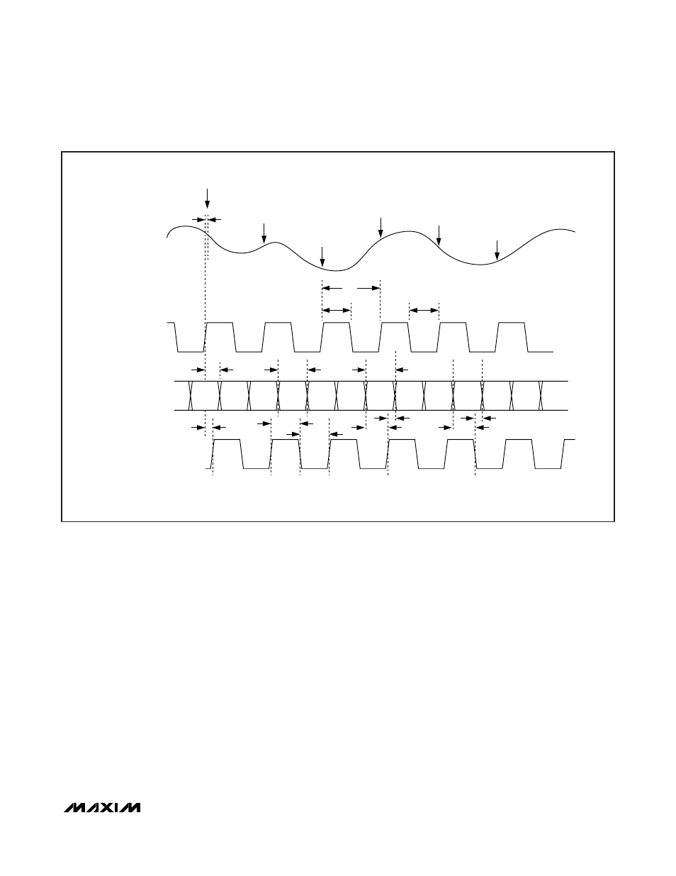
System Timing Requirements
Figures 9 and 10 depict the relationship between the
clock input and output, analog input, sampling event,
and data output. The MAX19515 samples on the rising
edge of the sampling clock. Output data is valid on the
next rising edge of DCLK after a nine-clock internal
latency. For applications where the clock is divided, the
sample clock is the divided internal clock derived from:
[(CLK+ - CLK-)/DIVIDER]
Synchronization
When using the clock divider, the phase of the internal
clock can be different than that of the FPGA, microcon-
troller, or other MAX19515s in the system. There are
two mechanisms to synchronize the internal clock: slip
synchronization and edge synchronization. Select the
synchronization mode using SYNC_MODE (bit 2) in the
Clock Divide/Data Format/Test Pattern register (06h)
and drive the SYNCIN input high to synchronize.
Slip Synchronization Mode, SYNC_MODE = 0
(default): On the third rising edge of the input clock
(CLK) after the rising edge of SYNC (provided set-up
and hold times are met), the divided output is forced to
skip a state transition (Figure 11).
Edge Synchronization Mode, SYNC_MODE = 1: On
the third rising edge of the input clock (CLK) after the
rising edge of SYNC (provided set-up and hold times
are met), the divided output is forced to state 0. A divid-
ed clock rising edge occurs on the fourth (/2 mode) or
fifth (/4 mode) rising edge of CLK, after a valid rising
edge of SYNC (Figure 12).
DCLK
DATA, DOR
SAMPLE CLOCK
n-9
CHA
CHB
n-9
n-8
CHA
CHB
n-8
CHB
n-10
n-7
CHA
CHB
n-7
n-6
CHA
CHB
n-6
n-5
CHA
CHB
n-5
n-4
CHA
CHB
n-4
MUX OUTPUT MODE
IN_
SAMPLING
INSTANT
SAMPLING
INSTANT
SAMPLING
INSTANT
SAMPLING
INSTANT
SAMPLING
INSTANT
SAMPLING
INSTANT
t
AD
n
n+1
n+2
n+4
n+5
n+3
t
CH
t
CL
SAMPLE ON RISING EDGE
t
DC
t
DD
t
CHA
t
DCH
t
SETUP
t
HOLD
t
HOLD
t
DCL
t
SETUP
t
CHB
SAMPLE CLOCK IS THE DERIVED CLOCK FROM (CLK+ - CLK-)/CLOCK DIVIDER, IN_ = IN_+ - IN_-.
MUX_CH (BIT 2, OUTPUT FORMAT 01h) DETERMINES THE OUTPUT BUS AND WHICH CHANNEL DATA IS PRESENTED.
t
CLK
Figure 10. Multiplexed Output Mode Timing