Table 1. parallel-interface pin functionality – Rainbow Electronics MAX19515 User Manual
Page 15
MAX19515
Dual-Channel, 10-Bit, 65Msps ADC
______________________________________________________________________________________
15
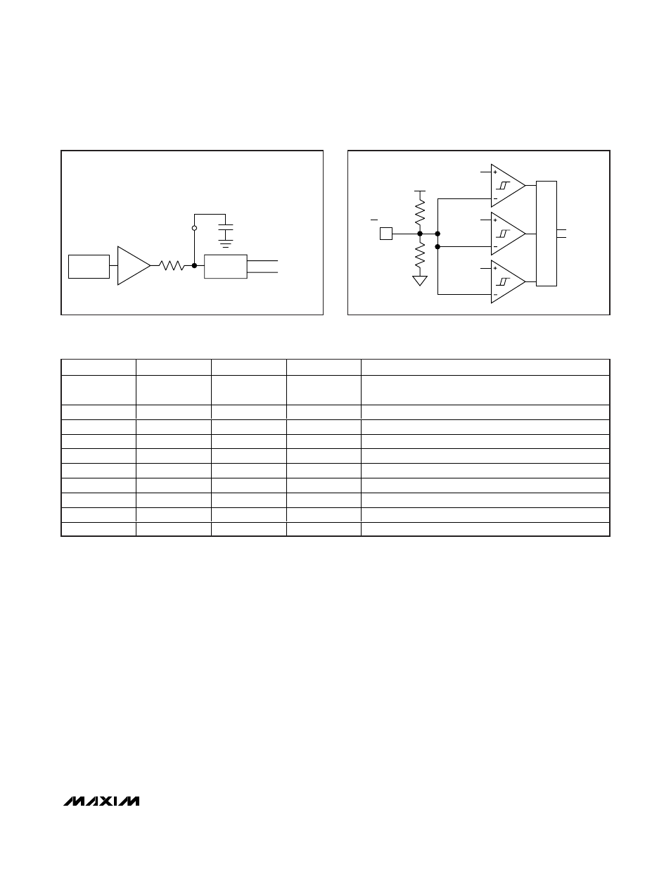
Reference Input/Output (REFIO)
REFIO adjusts the reference potential, which, in turn,
adjusts the full-scale range of the ADC. Figure 4 shows
a simplified schematic of the reference system. An
internal bandgap voltage generator provides an internal
reference voltage. The bandgap potential is buffered
and applied to REFIO through a 10kΩ resistor. Bypass
REFIO with a 0.1µF capacitor to AGND. The bandgap
voltage is applied to a scaling and level-shift circuit,
which creates internal reference potentials that estab-
lish the full-scale range of the ADC. Apply an external
voltage on REFIO to trim the ADC full scale. The allow-
able adjustment range is +5/-15%. The REFIO-to-ADC
gain transfer function is:
V
FS
= 1.5 x [V
REFIO
/1.25] Volts
Programming and Interface
There are two ways to control the MAX19515 operating
modes. Full feature selection is available using the SPI
interface, while the parallel interface offers a limited set
of commonly used features. The programming mode is
selected using the SPEN input. Drive SPEN low for SPI
interface; drive SPEN high for parallel interface.
Parallel Interface
The parallel interface offers a pin-programmable inter-
face with a limited feature set. Connect SPEN to AVDD
to enable the parallel interface. See Table 1 for pin
functionality; see Figure 5 for a simplified parallel-inter-
face input schematic.
BANDGAP
REFERENCE
BUFFER
1.250V
REFIO
INTERNAL GAIN—BYPASS REFIO
EXTERNAL GAIN CONTROL—DRIVE REFIO
SCALE AND
LEVEL SHIFT
INTERNAL REFERENCE
(CONTROLS ADC GAIN)
10k
Ω
0.1
μF
EXTERNAL BYPASS
Figure 4. Simplified Reference Schematic
36k
Ω
156k
Ω
CS
SCLK
SDIN
AVDD
29/32 AVDD
DECODER
TO
CONTROL
LOGIC
23/32 AVDD
3/32 AVDD
Figure 5. Simplified Parallel-Interface Input Schematic
SPEN
SDIN/FORMAT
SCLK/DIV
CS/OUTSEL
DESCRIPTION
0
SDIN
SCLK
CS
SPI interface active. Features are programmed through the
serial port (see the Serial Programming Interface section).
1
0
X
X
Two’s complement
1
AVDD
X
X
Offset binary
1
Unconnected
X
X
Gray code
1
X
0
X
Clock divide-by-1
1
X
AVDD
X
Clock divide-by-2
1
X
Unconnected
X
Clock divide-by-4
1
X
X
0
CMOS (dual bus)
1
X
X
AVDD
MUX CMOS (channel A data bus)
1
X
X
Unconnected
MUX CMOS (channel B data bus)
Table 1. Parallel-Interface Pin Functionality
X = Don’t care.