Detailed description, Pin description (continued) – Rainbow Electronics MAX19515 User Manual
Page 13
MAX19515
Dual-Channel, 10-Bit, 65Msps ADC
______________________________________________________________________________________
13
Detailed Description
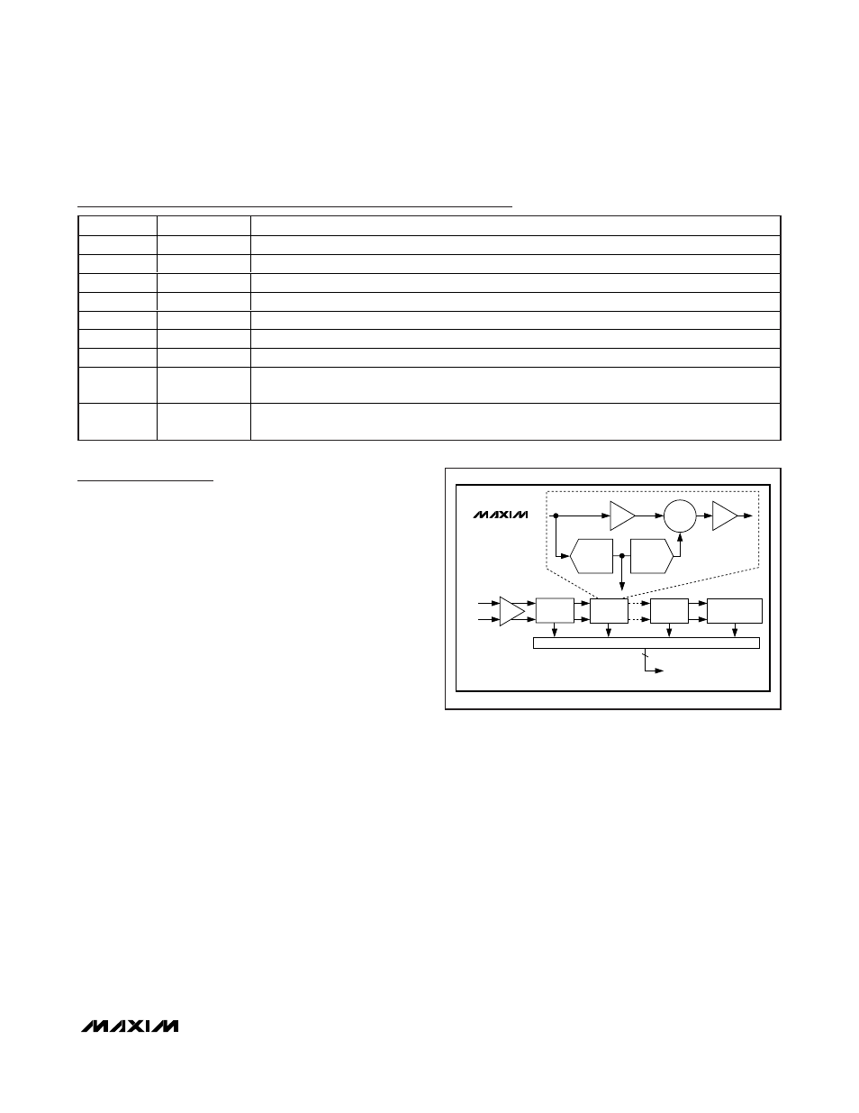
The MAX19515 uses a 10-stage, fully differential,
pipelined architecture (Figure 1) that allows for high-
speed conversion while minimizing power consump-
tion. Samples taken at the inputs move progressively
through the pipeline stages every half clock cycle.
From input to output the total latency is 9 clock cycles.
Each pipeline converter stage converts its input voltage
to a digital output code. At every stage, except the last,
the error between the input voltage and the digital out-
put code is multiplied and passed on to the next
pipeline stage. Digital error correction compensates for
ADC comparator offsets in each pipeline stage and
ensures no missing codes. Figure 2 shows the
MAX19515 functional diagram.
Analog Inputs and Common-Mode
Reference
Apply the analog input signal to the analog inputs
(INA+/INA- or INB+/INB-), which are connected to the
input sampling switch (Figure 3). When the input sam-
pling switch is closed, the input signal is applied to the
sampling capacitors through the input switch resistance.
The input signal is sampled at the instant the input
switch opens. The pipeline ADC processes the sampled
voltage and the digital output result is available 9 clock
cycles later. Before the input switch is closed to begin
the next sampling cycle, the sampling capacitors are
reset to the input common-mode potential.
Common-mode bias can be provided externally or
internally through 2kΩ resistors. In DC-coupled applica-
tions, the signal source provides the external bias and
the bias current. In AC-coupled applications, the input
current is supplied by the common-mode input voltage.
For example, the input current can be supplied through
the center tap of a transformer secondary winding.
Alternatively, program the appropriate internal register
through the serial-port interface to supply the input DC
current through internal 2kΩ resistors (Figure 3). When
the input current is supplied through the internal resis-
tors, the input common-mode potential is reduced by
the voltage drop across the resistors. The common-
mode input reference voltage can be adjusted through
programmable register settings from 0.45V to 1.35V in
0.15V increments. The default setting is 0.90V. Use this
feature to provide a common-mode output reference to
a DC-coupled driving circuit.
Pin Description (continued)
PIN
NAME
FUNCTION
40
D7A
Channel A Three-State Digital Output, Bit 7
41
D8A
Channel A Three-State Digital Output, Bit 8
42
D9A
Channel A Three-State Digital Output, Bit 9 (MSB)
43
DORA
Channel A Data Over Range
44
DCLKA
Channel A Data Clock
45
SDIN/FORMAT
SPI Data Input/Format. Serial-data input when
SPEN is low. Output data format when SPEN is high.
46
SCLK/DIV
Serial Clock/Clock Divider. Serial clock when
SPEN is low. Clock divider when SPEN is high.
47
CS/OUTSEL
Serial-Port Select/Data Output Mode. Serial-port select when
SPEN is low. Data output mode
selection when
SPEN is high.
—
EP
Exposed Pad. Internally connected to GND. Connect to a large ground plane to maximize thermal
performance.
MAX19515
Σ
+
−
DIGITAL ERROR CORRECTION
FLASH
ADC
x2
DAC
STAGE 2
IN_+
IN_-
STAGE 1
STAGE 9
STAGE 10
END OF PIPELINE
D0_ THROUGH D9_
Figure 1. Pipeline Architecture—Stage Blocks