Applications information – Rainbow Electronics MAX9552 User Manual
Page 7
MAX9550/MAX9551/MAX9552
High-Current VCOM Drive Buffers
for TFT LCDs
_______________________________________________________________________________________
7
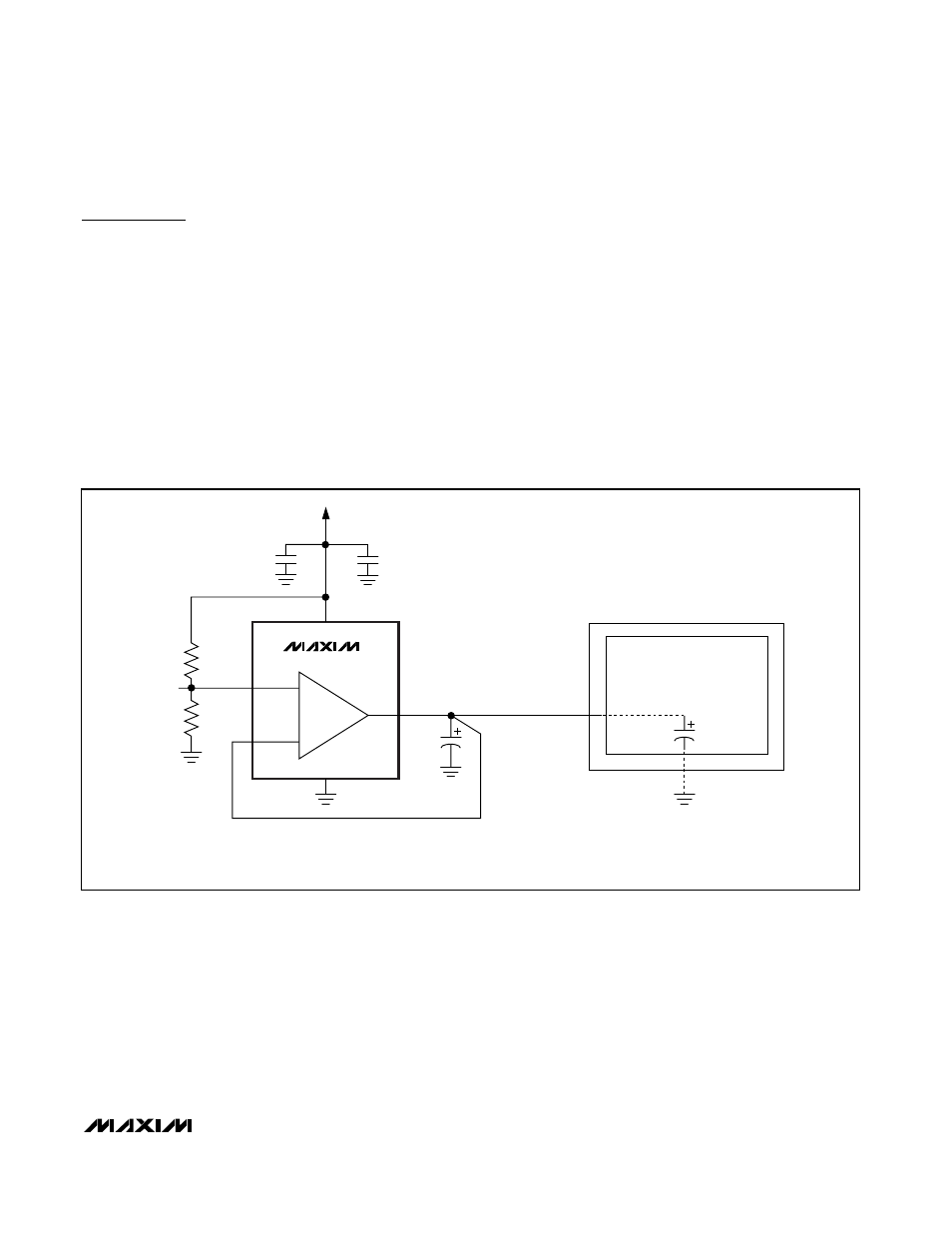
Applications Information
Output Load Capacitor
The output load capacitor must have a low ESR value
(50mΩ or lower) and it must be placed as close as pos-
sible to the OUT pin to ensure buffer stability (see
Figure 2). Ceramic capacitors are an excellent choice.
Power Supplies and Bypass Capacitors
The MAX9550/MAX9551/MAX9552 operate from a 6V to
20V single supply, or from ±3V to ±10V dual supplies.
Proper supply bypassing ensures stability while driving
high transient loads. The MAX9550/MAX9551/MAX9552
require minimum 4.7µF (C1) and 0.1µF (C2) power-sup-
ply bypass capacitors placed as close as possible to
the power-supply pin (V
DD
). See Figure 2. For dual-
supply operation, use 4.7µF and 0.1µF bypass capaci-
tors on both supplies (V
DD
and GND) with each
capacitor placed as close as possible to the V
DD
and
GND pins.
Layout and Grounding
The exposed paddle on the µMAX and TSSOP pack-
ages provides a low thermal resistance for heat dissi-
pation. Solder the exposed paddle to a ground plane
for best results. Do not route traces under these pack-
ages. For dual-supply operation, the exposed paddle
(EP) must be electrically connected to the negative
supply or it can be left unconnected.
MAX9550
16V
SUPPLY
*C1 = 4.7µF
C
L
= 1µF
*C2 = 0.1µF
*PLACE 4.7µF AND 0.1µF CAPACITORS AS CLOSE TO PIN AS POSSIBLE.
NOTE: PLACE C
L
AS CLOSE TO THE OUT PIN AS POSSIBLE
AND KELVIN SENSE THE FEEDBACK LOOP CONNECTION AS SHOWN.
IN+
OUT
V
OUT
TFT-LCD
CAPACITANCE
V
REF
V
DD
TFT LCD
IN-
GND
Figure 2. Typical TFT-LCD Backplane Drive Circuit