Applications hints – Rainbow Electronics ADC10738 User Manual
Page 24

Applications Hints
(Continued)
3 4 Optional Adjustments
3 4 1 Zero Error
The zero error of the A D converter relates to the location
of the first riser of the transfer function (see
Figure 1
) and
can be measured by grounding the minus input and applying
a small magnitude voltage to the plus input Zero error is the
difference between actual DC input voltage which is neces-
sary to just cause an output digital code transition from
000 0000 0000 to 000 0000 0001 and the ideal
LSB
value (
LSB e 1 22 mV for V
REF
e a
2 500V)
The zero error of the A D does not require adjustment If
the minimum analog input voltage value V
IN
(Min) is not
ground the effective ‘‘zero’’ voltage can be adjusted to a
convenient value The converter can be made to output an
all zeros digital code for this minimum input voltage by bias-
ing any minus input to V
IN
(Min) This is useful for either the
differential or pseudo-differential input channel configura-
tions
3 4 2 Full-Scale
The full-scale adjustment can be made by applying a differ-
ential input voltage which is 1
LSB down from the desired
analog full-scale voltage range and then adjusting the V
REF
voltage (V
REF
e
V
REF
a
– V
REF
b
) for a digital output code
changing from 011 1111 1110 to 011 1111 1111 In bipolar
signed operation this only adjusts the positive full scale er-
ror
3 4 3 Adjusting for an Arbitrary Analog Input
Voltage Range
If the analog zero voltage of the A D is shifted away from
ground (for example to accommodate an analog input sig-
nal which does not go to ground) this new zero reference
should be properly adjusted first A plus input voltage which
equals this desired zero reference plus
LSB is applied to
selected plus input and the zero reference voltage at the
corresponding minus input should then be adjusted to just
obtain the 000 0000 0000 to 000 0000 0001 code transition
The full-scale adjustment should be made with the proper
minus input voltage applied by forcing a voltage to the plus
input which is given by
V
IN
(a) f
s
adj e V
MAX
b
1 5
(V
MAX
b
V
MIN
)
2
n
(
where V
MAX
equals the high end of the analog input range
V
MIN
equals the low end (the offset zero) of the analog
range Both V
MAX
and V
MIN
are ground referred The V
REF
(V
REF
e
V
REF
a
b
V
REF
b
) voltage is then adjusted to pro-
vide a code change from 011 1111 1110 to 011 1111 1111
Note when using a pseudo-differential or differential multi-
plexer mode where V
REF
a
and V
REF
b
are placed within
the V
a
and GND range the individual values of V
REF
and
V
REF
b
do not matter only the difference sets the analog
input voltage span This completes the adjustment proce-
dure
3 5 The Input Sample and Hold
The ADC10731 2 4 8’s sample hold capacitor is imple-
mented in the capacitor array After the channel address is
loaded the array is switched to sample the selected positive
analog input The sampling period for the assigned positive
input is maintained for the duration of the acquisition time
(t
A
) 4 5 clock cycles
This acquisition window of 4 5 clock cycles is available to
allow the voltage on the capacitor array to settle to the posi-
tive analog input voltage Any change in the analog voltage
on a selected positive input before or after the acquisition
window will not effect the A D conversion result
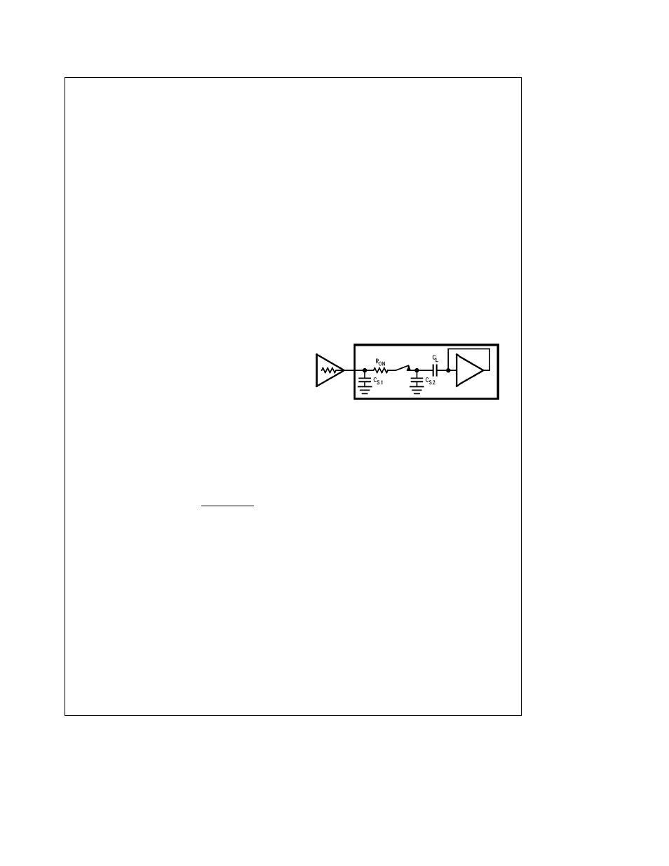
In the simplest case the array’s acquisition time is deter-
mined by the R
ON
(3 kX) of the multiplexer switches the
stray input capacitance C
S1
(3 5 pF) and the total array (C
L
)
and stray (C
S2
) capacitance (48 pF) For a large source
resistance the analog input can be modeled as an RC net-
work as shown in
Figure 14
The values shown yield an
acquisition time of about 1 1 ms for 10-bit unipolar or 10-bit
plus sign accuracy with a zero-to-full-scale change in the
input voltage External source resistance and capacitance
will lengthen the acquisition time and should be accounted
for Slowing the clock will lengthen the acquisition time
thereby allowing a larger external source resistance
TL H 11390 – 25
FIGURE 14 Analog Input Model
The signal-to-noise ratio of an ideal A D is the ratio of the
RMS value of the full scale input signal amplitude to the
value of the total error amplitude (including noise) caused
by the transfer function of the ideal A D An ideal 10-bit plus
sign A D converter with a total unadjusted error of 0 LSB
would have a signal-to-(noise a distortion) ratio of about 68
dB which can be derived from the equation
S (N a D) e 6 02(n) a 1 8
where S (N a D) is in dB and n is the number of bits
24
