Clearing the dac, Applications information – Rainbow Electronics MAX5144 User Manual
Page 8
MAX5141–MAX5144
+3V/+5V, Serial-Input,
Voltage-Output, 14-Bit DACs
8
_______________________________________________________________________________________
to a standard R-2R ladder, allowing unbuffered opera-
tion in medium-load applications.
The MAX5142/MAX5144 provide matched bipolar offset
resistors, which connect to an external op amp for bipo-
lar output swings (Figure 2b).
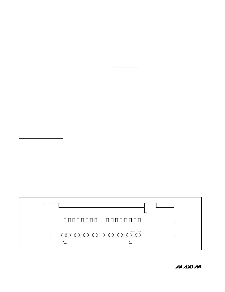
Digital Interface
The MAX5141–MAX5144 digital interface is a standard
3-wire connection compatible with SPI/QSPI/
MICROWIRE interfaces. The chip-select input (CS)
frames the serial data loading at the data-input pin
(DIN). Immediately following CS’s high-to-low transition,
the data is shifted synchronously and latched into the
input register on the rising edge of the serial clock input
(SCLK). After 16 bits (14 data bits, plus two subbits set
to zero) have been loaded into the serial input register,
it transfers its contents to the DAC latch on CS’s low-to-
high transition (Figure 3). Note that if CS is not kept low
during the entire 16 SCLK cycles, data will be corrupt-
ed. In this case, reload the DAC latch with a new 16-bit
word.
Clearing the DAC
A 20ns (min) logic low pulse on CLR asynchronously
clears the DAC buffer to code 0 in the MAX5141/
MAX5143 and to code 8192 in the MAX5142/MAX5144.
External Reference
The MAX5141–MAX5144 operate with external voltage
references from +2V to V
DD
. The reference voltage
determines the DAC’s full-scale output voltage.
Power-On Reset
The power-on reset circuit sets the output of the
MAX5141/MAX5143 to code 0 and the output of the
MAX5142/MAX5144 to code 8192 when V
DD
is first
applied. This ensures that unwanted DAC output volt-
ages will not occur immediately following a system
power-up, such as after a loss of power.
Applications Information
Reference and Ground Inputs
The MAX5141–MAX5144 operate with external voltage
references from +2V to V
DD
, and maintain 14-bit perfor-
mance if certain guidelines are followed when selecting
and applying the reference. Ideally, the reference’s
temperature coefficient should be less than 0.5ppm/°C to
maintain 14-bit accuracy to within 1LSB over the -40°C to
+85°C extended temperature range. Since this converter
is designed as an inverted R-2R voltage-mode DAC, the
input resistance seen by the voltage reference is code
dependent. In unipolar mode, the worst-case input-resis-
tance variation is from 11.5k
Ω (at code 2155 hex) to
200k
Ω (at code 0000 hex). The maximum change in load
current for a +2.5V reference is +2.5V / 11.5k
Ω = 217µA;
therefore, the required load regulation is 28ppm/mA for a
maximum error of 0.1LSB. This implies a reference out-
put impedance of less than 72m
Ω. In addition, the sig-
nal-path impedance from the voltage reference to the
reference input must be kept low because it contributes
directly to the load-regulation error.
The requirement for a low-impedance voltage reference
is met with capacitor bypassing at the reference inputs
and ground. A 0.1µF ceramic capacitor with short leads
between REF and GND provides high-frequency
bypassing. A surface-mount ceramic chip capacitor is
preferred because it has the lowest inductance. An
additional 1µF between REF and GND provides low-fre-
quency bypassing. A low-ESR tantalum, film, or organic
semiconductor capacitor works well. Leaded capaci-
tors are acceptable because impedance is not as criti-
;
;
;;
CS
SCLK
DIN
MSB
LSB
D13
D6
D5 D4 D3 D2 D1 D0
S1 S0
SUB-BITS
DAC
UPDATED
D12 D11 D10 D9 D8 D7
Figure 3. MAX5141–MAX5144 3-Wire Interface Timing Diagram