Chip information, Functional diagrams – Rainbow Electronics MAX5144 User Manual
Page 10

MAX5141–MAX5144
+3V/+5V, Serial-Input,
Voltage-Output, 14-Bit DACs
10
______________________________________________________________________________________
Unipolar Configuration
Figure 2a shows the MAX5141–MAX5144 configured for
unipolar operation with an external op amp. The op amp
is set for unity gain, and Table 1 lists the codes for this
circuit. Bipolar MAX5142/MAX5144 can also be used in
unipolar configuration by connecting RFB and INV to
REF. This allows the DAC to power up to midscale.
Bipolar Configuration
Figure 2b shows the MAX5141–MAX5144 configured
for bipolar operation with an external op amp. The op
amp is set for unity gain with an offset of -1/2V
REF
.
Table 2 shows the offset binary codes for this circuit
(less than 0.25 inches).
Power-Supply Bypassing and
Ground Management
Bypass V
DD
with a 0.1µF ceramic capacitor connected
between V
DD
and GND. Mount the capacitor with short
leads close to the device (less than 0.25 inches).
Table 1. Unipolar Code Table
Table 2. Bipolar Code Table
V
REF ✕
(1 / 16,384)
0000 0000 0000 01
V
REF ✕
(8192 / 16,384) = 1/2V
REF
1000 0000 0000 00
V
REF ✕
(16,383 / 16,384)
1111 1111 1111 11
ANALOG OUTPUT, V
OUT
MSB LSB
DAC LATCH CONTENTS
-V
REF ✕
(8192 / 8192) = -V
REF
0000 0000 0000 00
-V
REF ✕
(1 / 8192)
0111 1111 1111 11
0V
1000 0000 0000 00
+V
REF ✕
(1 / 8192)
1000 0000 0000 01
+V
REF ✕
(8191 / 8192)
1111 1111 1111 11
ANALOG OUTPUT, V
OUT
MSB LSB
DAC LATCH CONTENTS
Chip Information
TRANSISTOR COUNT: 2800
PROCESS: BiCMOS
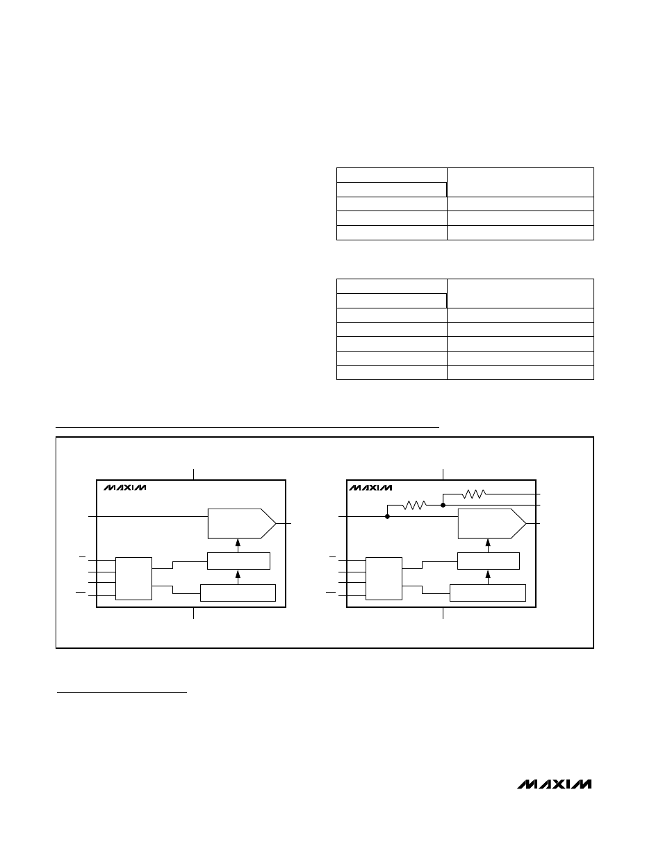
Functional Diagrams
GND
V
DD
OUT
CLR
DIN
SCLK
CS
REF
MAX5141
MAX5143
14-BIT DAC
CONTROL
LOGIC
14-BIT DATA LATCH
SERIAL INPUT REGISTER
GND
V
DD
OUT
CLR
DIN
SCLK
CS
REF
14-BIT DAC
CONTROL
LOGIC
14-BIT DATA LATCH
SERIAL INPUT REGISTER
RFB
INV
MAX5142
MAX5144
