Pin descriptions – Rainbow Electronics MAX5144 User Manual
Page 6
MAX5141–MAX5144
+3V/+5V, Serial-Input,
Voltage-Output, 14-Bit DACs
6
_______________________________________________________________________________________
Pin Descriptions
PIN
MAX5141
MAX5143
MAX5142
MAX5144
NAME
FUNCTION
1
1
REF
Voltage Reference Input
2
2
CS
Chip-Select Input
3
3
SCLK
Serial Clock Input. Duty cycle must be between 40% and 60%.
4
4
DIN
Serial Data Input
5
5
CLR
Clear Input. Logic low asynchronously clears the DAC to code 0
(MAX5141/MAX5143) or code 8192 (MAX5142/MAX5144).
6
6
OUT
DAC Output Voltage
—
7
INV
Junction of Internal Scaling Resistors. Connect to external op amp’s inverting input in
bipolar mode.
—
8
RFB
Feedback Resistor. Connect to external op amp’s output in bipolar mode.
7
9
V
DD
Supply Voltage. Use +3V for MAX5143/MAX5144 and +5V for MAX5141/MAX5142.
8
10
GND
Ground
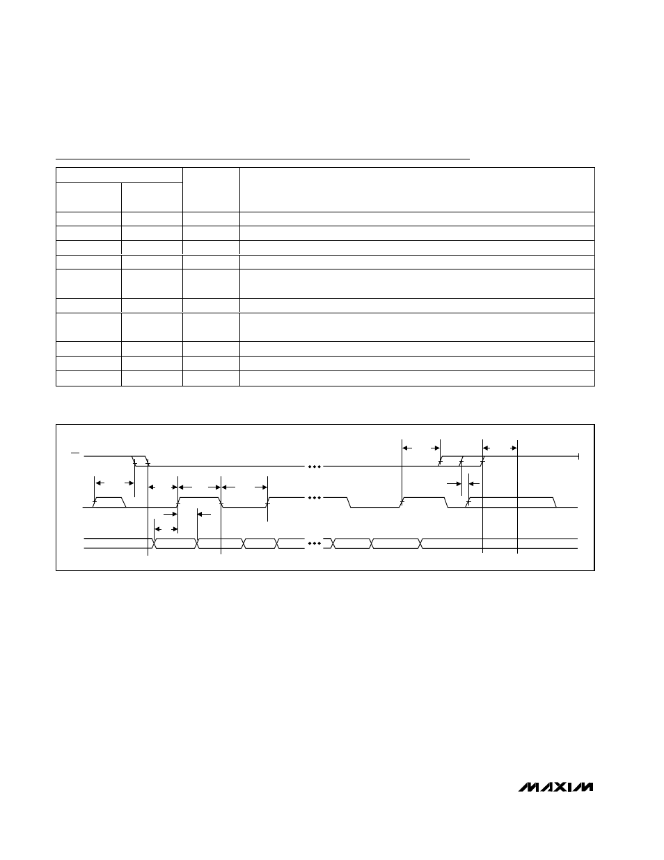
;;
;;
;;;;;;;;;
;;
;;
t
CSHO
t
CH
t
CSSO
t
CL
t
DH
t
DS
t
CSH1
t
CSS1
t
LDACS
CS
SCLK
DIN
D13 D12
S0
Figure 1. Timing Diagram
- MAX5151 (16 pages)
- MAXQ3108 (64 pages)
- MAX5661 (39 pages)
- MAX6691 (7 pages)
- MAX5362 (12 pages)
- ADC10158 (26 pages)
- MAX8922L (14 pages)
- MAX8596Z (8 pages)
- MAX7491 (18 pages)
- MAX15040 (15 pages)
- MAX5177 (16 pages)
- ADC08138 (22 pages)
- MAX5961 (42 pages)
- T89C51RD2 (86 pages)
- MAX16055 (9 pages)
- MAX6659 (17 pages)
- ADC0820 (20 pages)
- MAX6678 (19 pages)
- MAX8884Z (15 pages)
- MAX16915 (9 pages)
- MAX8620 (18 pages)
- MAX6670 (8 pages)
- MAX8760 (39 pages)
- W78C32C (14 pages)
- MX7533 (8 pages)
- MAX8727 (13 pages)
- MAX9053 (15 pages)
- W78C54 (16 pages)
- MAX8614B (15 pages)
- W90N740 (219 pages)
- MAX6626 (13 pages)
- ADC10738 (30 pages)
- MAX17000 (31 pages)
- MAX5051 (21 pages)
- MAXQ1004 (18 pages)
- MAX6871 (51 pages)
- MX7847 (12 pages)
- MAX6608 (6 pages)
- MAX17083 (15 pages)
- MAX6641 (17 pages)
- MAX5251 (16 pages)
- MAX6338 (8 pages)
- MAX6690 (16 pages)
- MAX8668 (18 pages)