Timing characteristics, Electrical characteristics (continued) – Rainbow Electronics MAX5144 User Manual
Page 3
MAX5141–MAX5144
+3V/+5V, Serial-Input,
Voltage-Output, 14-Bit DACs
_______________________________________________________________________________________
3
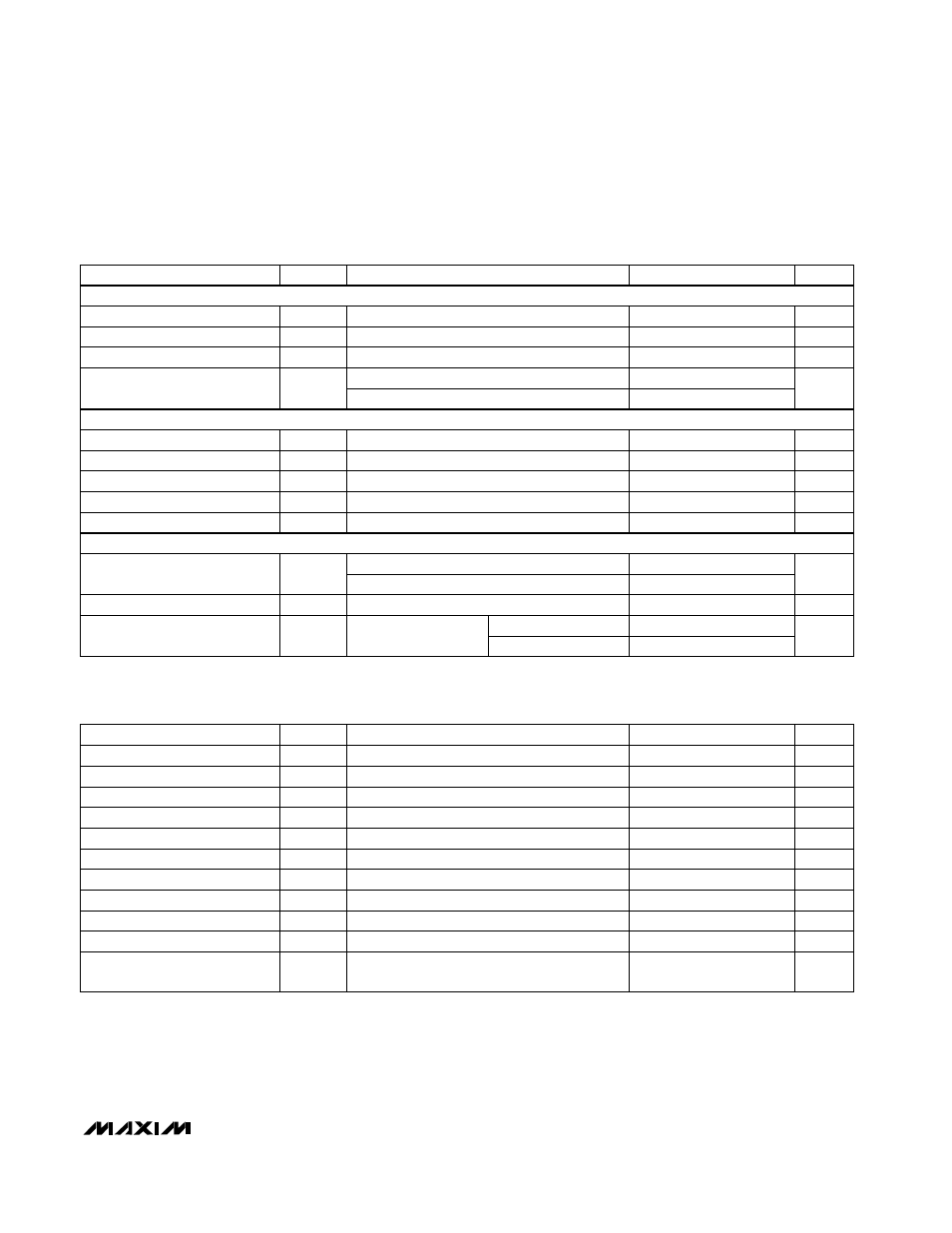
TIMING CHARACTERISTICS
(V
DD
= +2.7V to +3.3V (MAX5143/MAX5144), V
DD
= +4.5V to +5.5V (MAX5141/MAX5142), V
REF
= +2.5V, GND = 0, CMOS inputs,
T
A
= T
MIN
to T
MAX
, unless otherwise noted. Typical values are at T
A
= +25°C.) (Figure 1)
Note 1: Gain error tested at V
REF
= +2.0V, +2.5V, and +3.0V (MAX5143/MAX5144) or V
REF
= +2.0V, +2.5V, +3.0V, and +5.0V
(MAX5141/MAX5142).
Note 2: R
OUT
tolerance is typically ±20%.
Note 3: Min/max range guaranteed by gain-error test. Operation outside min/max limits will result in degraded performance.
Note 4: Reference input resistance is code dependent, minimum at 2155 hex in unipolar mode, 1155 hex in bipolar mode.
Note 5: Slew-rate value is measured from 10% to 90%.
Note 6: Guaranteed by design. Not production tested.
Note 7: Guaranteed by power-supply rejection test and Timing Characteristics.
Code = 3FFF hex
All digital inputs at
V
DD
or GND
All digital inputs at V
DD
or GND
MAX5143/MAX5144
Code = 0000 hex, V
REF
= 1V
P-P
at 100kHz
Code = 0000 hex
Code = 3FFF hex
(Note 6)
CONDITIONS
mW
0.36
PD
Power Dissipation
mA
0.12
0.20
I
DD
Positive Supply Current
V
2.7
3.6
V
DD
Positive Supply Range (Note 7)
V
0.15
V
H
Hysteresis Voltage
pF
3
10
C
IN
Input Capacitance
mV
P-P
1
MHz
1
BW
Reference -3dB Bandwidth
µA
±1
I
IN
Input Current
V
0.8
V
IL
Input Low Voltage
V
2.4
V
IH
Input High Voltage
Reference Feedthrough
dB
92
SNR
Signal-to-Noise Ratio
70
pF
170
C
INREF
Reference Input Capacitance
UNITS
MIN
TYP
MAX
SYMBOL
PARAMETER
(Note 6)
CONDITIONS
µs
20
V
DD
High to CS Low
(Power-Up Delay)
ns
20
t
CL
SCLK Pulse Width Low
ns
20
t
CH
MHz
25
f
CLK
SCLK Frequency
SCLK Pulse Width High
ns
20
t
CLW
CLR Pulse Width Low
ns
0
t
DH
DIN to SCLK High Hold
ns
15
t
DS
DIN to SCLK High Setup
ns
15
t
CSS0
CS Low to SCLK High Setup
ns
15
t
CSS1
CS High to SCLK High Setup
ns
35
t
CSH0
SCLK High to CS Low Hold
ns
20
t
CSH1
SCLK High to CS High Hold
UNITS
MIN
TYP
MAX
SYMBOL
PARAMETER
ELECTRICAL CHARACTERISTICS (continued)
(V
DD
= +3V (MAX5143/MAX5144) or +5V (MAX5141/MAX5142), V
REF
= +2.5V, T
A
= T
MIN
to T
MAX
, C
L
= 10pF, GND = 0, RL =
∞,
unless otherwise noted. Typical values are at T
A
= +25°C.)
0.60
MAX5141/MAX5142
MAX5143/MAX5144
MAX5141/MAX5142
4.5
5.5
DYNAMIC PERFORMANCE—REFERENCE SECTION
STATIC PERFORMANCE—DIGITAL INPUTS
POWER SUPPLY