Typical operating characteristics (continued), Pin description – Rainbow Electronics MAX16915 User Manual
Page 5

Ideal Diode, Reverse-Battery, and Overvoltage Protection
Switch/Limiter Controllers with External MOSFETs
MAX16914/MAX16915
_______________________________________________________________________________________ 5
Typical Operating Characteristics (continued)
(V
CC
= 14V, V
SHDN
= 14V, MAX16914/MAX16915 Evaluation Kit, T
A
= +25NC, unless otherwise noted.)
Pin Description
PIN
NAME
FUNCTION
1
V
CC
Positive Supply Input Voltage. Bypass V
CC
to GND with a 0.1FF or greater ceramic capacitor.
2
GATE1
Gate-Driver Output. Connect GATE1 to the gate of an external p-channel FET pass switch to pro-
vide low drain-to-source voltage drop, reverse voltage protection, and back-charge prevention.
3
SENSE IN
Differential Voltage Sense Input (Input Side of IC). Used with SENSE OUT to provide back-charge
prevention when the SENSE IN voltage falls below the SENSE OUT voltage by 25mV.
4
SHDN
Active-Low Shutdown/Wake Input. Drive SHDN high to turn on the voltage detectors. GATE2 is
shorted to V
CC
when SHDN is low. SHDN is internally pulled to GND through a 0.5FA current sink.
Connect SHDN to V
CC
for always-on operation.
5
OV
Open-Drain Overvoltage Indicator Output. Connect a pullup resistor from OV to a positive supply
such as V
CC
. OV is pulled low when the voltage at SET exceeds the internal threshold.
6
GND
Ground
7
SET
Controller Overvoltage Threshold Programming Input. Connect SET to the center of an external
resistive divider network between TERM and GND to adjust the desired overvoltage switch-off or
limiter threshold.
8
TERM
Voltage-Divider Termination Output. TERM is internally connected to SENSE OUT in the MAX16915
and to V
CC
in the MAX16914. TERM is high impedance when SHDN is low, forcing the current to
zero in the resistor-divider connected to TERM.
9
SENSE OUT
Differential Voltage Sense Input (Output Side Of IC). Used with SENSE IN to provide back-charge
prevention when the SENSE IN voltage falls below the SENSE OUT voltage by 25mV.
10
GATE2
Gate-Driver Output. Connect GATE2 to the gate of an external p-channel FET pass switch. GATE2
is driven low during normal operation and quickly regulated or shorted to V
CC
during an overvolt-
age condition. GATE2 is shorted to V
CC
when SHDN is low.
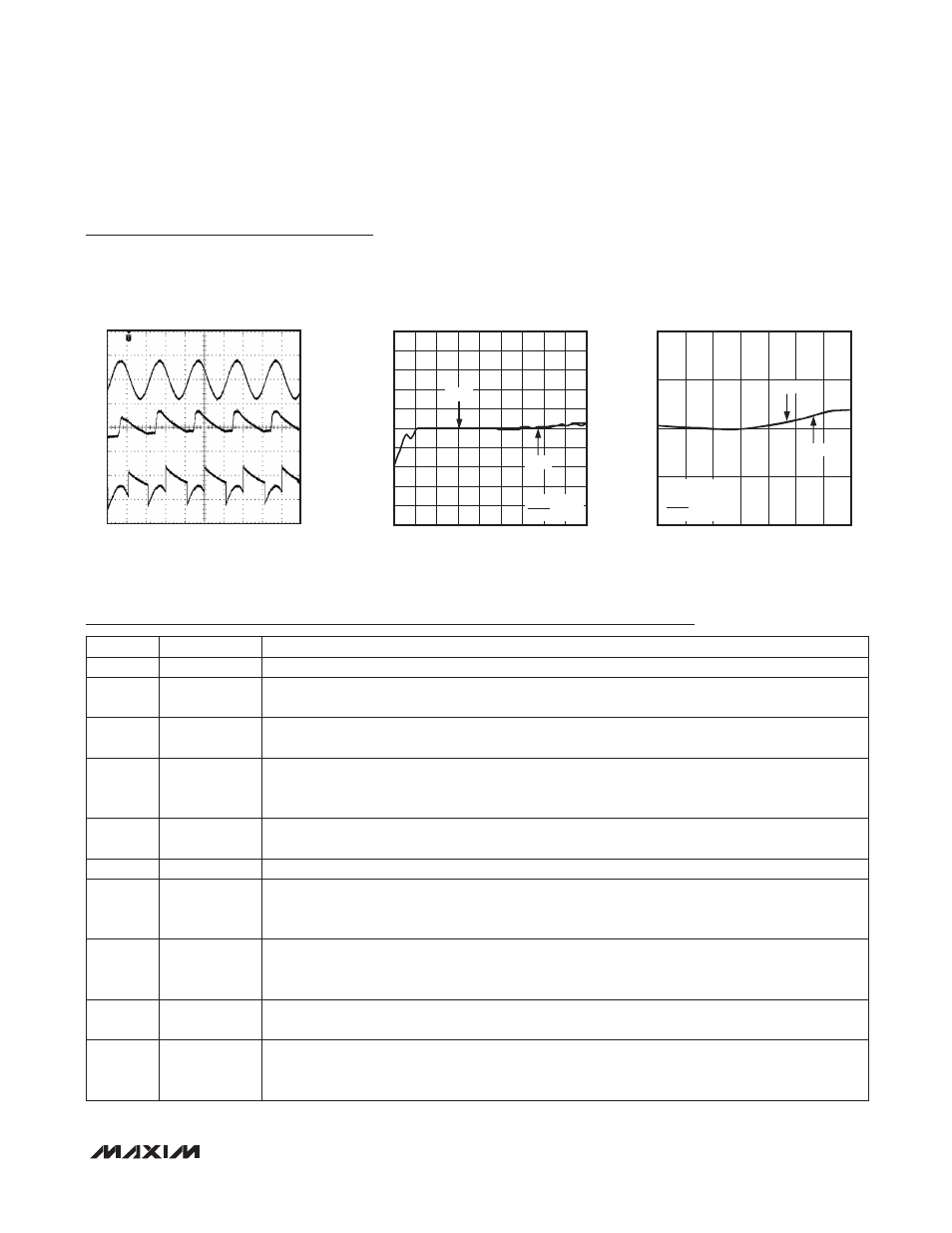
BACK-CHARGE RESPONSE
MAX16914 toc10
1.0µs/div
2.2µF INPUT CAPACITOR, 400I
INPUT RESISTOR, 22µF OUTPUT CAPACITOR
V
CC
5V/div
V
OUT
5V/div
0V
5V
5V
V
GATE1
5V/div
V
CC
- V
GATE_
vs. INPUT VOLTAGE
MAX16914 toc11
SUPPLY VOLTAGE (V)
GATE DRIVE VOLTAGE (V)
40.5
36.0
27.0 31.5
13.5 18.0 22.5
9.0
1.5
3.0
4.5
6.0
7.5
9.0
10.5
12.0
13.5
15.0
0
4.5
44.0
GATE1
GATE2
SET = GND
SHDN = HIGH
GATE-DRIVE VOLTAGE
vs. TEMPERATURE
MAX16914 toc12
TEMPERATURE (NC)
GATE-DRIVE VOLTAGE (V)
110
85
60
35
10
-15
6.3
6.4
6.5
6.6
6.2
-40
125
GATE1
GATE2
V
CC
= 14V
SET = GND
SHDN = HIGH
