Electrical characteristics, Absolute maximum ratings – Rainbow Electronics MAX16915 User Manual
Page 2
Ideal Diode, Reverse-Battery, and Overvoltage Protection
Switch/Limiter Controllers with External MOSFETs
MAX16914/MAX16915
2 ______________________________________________________________________________________
Stresses beyond those listed under “Absolute Maximum Ratings” may cause permanent damage to the device. These are stress ratings only, and functional
operation of the device at these or any other conditions beyond those indicated in the operational sections of the specifications is not implied. Exposure to absolute
maximum rating conditions for extended periods may affect device reliability.
V
CC
, SENSE OUT, TERM, SHDN, OV to GND for
P
400ms .............................................................-0.3V to +44V
V
CC
, SENSE OUT, TERM, SHDN, OV to GND
for P 90s .............................................................-0.3V to +28V
V
CC
, SENSE OUT, TERM, SHDN, OV to GND .....-0.3V to +20V
SENSE IN to GND for P 2ms ..................................-75V to +44V
SENSE IN to GND for P 90s ..................................-18V to +44V
SENSE IN to GND .................................................-0.3V to +20V
GATE1, GATE2 to V
CC
..........................................-16V to +0.3V
GATE1, GATE2 to GND ........................... -0.3V to (V
CC
+ 0.3V)
SET to GND .............................................................-0.3V to +8V
Continuous Power Dissipation (T
A
= +70NC)
10-Pin FMAX (derate 8.8mW/NC above T
A
= +70NC)
(Note 1) .......................................................................707mW
Operating Temperature Range ........................ -40NC to +125NC
Junction Temperature .....................................................+150NC
Storage Temperature Range ............................ -65NC to +150NC
Lead Temperature (soldering, 10s) ................................+300NC
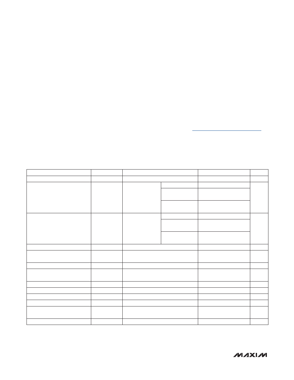
ELECTRICAL CHARACTERISTICS
(V
CC
= 14V, C
GATE1
= 32nF, C
GATE2
= 32nF,
SHDN
= high, T
A
= -40NC to +125NC, unless otherwise noted. Typical
values are at T
A
= +25NC.) (Note 2)
ABSOLUTE MAXIMUM RATINGS
Note 1:
Package thermal resistances were obtained using the method described in JEDEC specification JESD51-7, using a four-
layer board. For detailed information on package thermal considerations, refer to
.
PARAMETER
SYMBOL
CONDITIONS
MIN
TYP
MAX
UNITS
Operating Voltage Range
V
CC
(Note 3)
4.5
19
V
Shutdown Supply Current
(I
SENSE IN
+ I
SENSE OUT
+ I
OV
+
I
SHDN
+ I
VCC
)
I
SHDN
SHDN = low,
V
SENSE OUT
= 0V,
V
TERM
= 0V
T
A
= +25NC
6.0
12
F
A
T
A
= +85NC (Note
3)
6.1
12
T
A
= +125NC
(Note 3)
6.2
12
Quiescent Supply Current
(I
SENSE IN
+ I
SENSE OUT
+ I
OV
+
I
SHDN
+ I
VCC
)
I
Q
SHDN = high
T
A
= +25NC
29
53
F
A
T
A
= +85NC (Note
3)
30
55
T
A
= +125NC
(Note 3)
31
57
V
CC
Undervoltage Lockout
V
UVLO
V
CC
rising, V
SET
= 1V , SHDN = high
4.06
4.35
V
V
CC
Undervoltage-Lockout
Hysteresis
8
%
SET Threshold Voltage
V
SETTH
V
SET
rising
-3%
+1.20
+3%
V
SET Threshold Voltage
Hysteresis
V
SETHY
4
%
SET Input Current
I
SET
V
SET
= 1V
0.02
0.2
F
A
SHDN Low Threshold
V
SHDNL
0.4
V
SHDN High Threshold
V
SHDNH
1.4
V
SHDN Pulldown Current
I
SHDN
V
SHDN
= 14V, internally pulled to GND
0.5
1.0
F
A
V
CC
to GATE Output Low
Voltage
V
GVCC1
V
CC
= 14V
6.25
7.5
8.5
V
V
CC
to GATE Clamp Voltage
V
GVCC2
V
CC
= 42V
14
V