1 0 functional description – Rainbow Electronics ADC0820 User Manual
Page 8
1 0 Functional Description
(Continued)
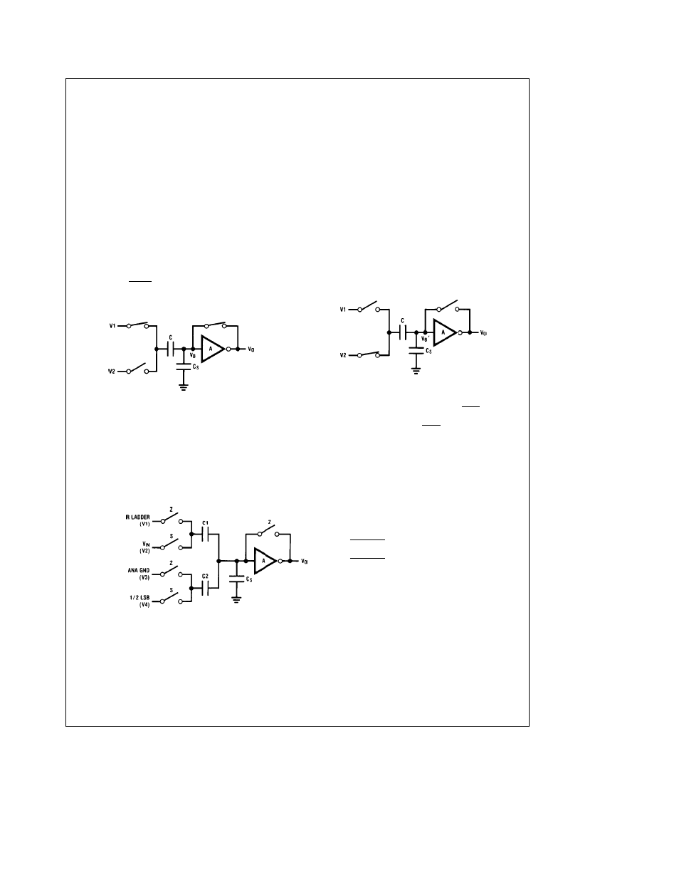
1 2 THE SAMPLED-DATA COMPARATOR
Each comparator in the ADC0820 consists of a CMOS in-
verter with a capacitively coupled input (
Figure 5
) Analog
switches connect the two comparator inputs to the input
capacitor (C) and also connect the inverter’s input and out-
put This device in effect now has one differential input pair
A comparison requires two cycles one for zeroing the com-
parator and another for making the comparison
In the first cycle one input switch and the inverter’s feed-
back switch (
Figure 5a
) are closed In this interval C is
charged to the connected input (V1) less the inverter’s bias
voltage (V
B
approximately 1 2V) In the second cycle (
Fig-
ure 5b
) these two switches are opened and the other (V2)
input’s switch is closed The input capacitor now subtracts
its stored voltage from the second input and the difference
is amplified by the inverter’s open loop gain The inverter’s
input (V
B
) becomes
V
B
b
(V1bV2)
C
CaC
S
and the output will go high or low depending on the sign of
V
B
b
V
B
TL H 5501 – 12
V
O
e
V
B
V on C
e
V1
b
V
B
C
S
e
stray input
node capacitor
V
B
e
inverter input
bias voltage
FIGURE 5a Zeroing Phase
The actual circuitry used in the ADC0820 is a simple but
important expansion of the basic comparator described
above By adding a second capacitor and another set of
switches to the input (
Figure 6
) the scheme can be expand-
ed to make dual differential comparisons In this circuit the
feedback switch and one input switch on each capacitor (Z
switches) are closed in the zeroing cycle A comparison is
then made by connecting the second input on each capaci-
tor and opening all of the other switches (S switches) The
change in voltage at the inverter’s input as a result of the
change in charge on each input capacitor will now depend
on both input signal differences
1 3 ARCHITECTURE
In the ADC0820 one bank of 15 comparators is used in
each 4-bit flash A D converter (
Figure 7
) The MS (most
significant) flash ADC also has one additional comparator to
detect input overrange These two sets of comparators op-
erate alternately with one group in its zeroing cycle while
the other is comparing
TL H 5501 – 13
V
B
b
V
B
e
(V2
b
V1)
C
C
a
C
S
V
O
e
b
A
C
a
C
S
CV2
b
CV1
V
O
is dependent on V2
b
V1
FIGURE 5b Compare Phase
FIGURE 5 Sampled-Data Comparator
TL H 5501 – 14
V
O
e
b
A
C1
a
C2
a
C
S
C1(V2
b
V1)
a
C2(V4
b
V3)
e
b
A
C1
a
C2
a
C
S
D
Q
C1
a
D
Q
C2
FIGURE 6 ADC0820 Comparator (from MS Flash ADC)
8