Ac electrical characteristics, Tri-state test circuits and waveforms – Rainbow Electronics ADC0820 User Manual
Page 4
AC Electrical Characteristics
(Continued) The following specifications apply for V
CC
e
5V t
r
e
t
f
e
20 ns
V
REF
(a)e5V V
REF
(b)e0V and T
A
e
25 C unless otherwise specified
Typ
Tested
Design
Parameter
Conditions
(Note 6)
Limit
Limit
Units
(Note 7)
(Note 8)
t
I
Internal Comparison Time
Pin 7eV
CC
(Figures 3b
and
4)
800
1300
ns
C
L
e
50 pF
t
1H
t
0H
TRI-STATE Control
R
L
e
1k C
L
e
10 pF
100
200
ns
(Delay from Rising Edge of RD to
Hi-Z State)
t
INTL
Delay from Rising Edge of
Pin 7 e V
CC
C
L
e
50 pF
WR to Falling Edge of INT
t
RD
l
t
I
(Figure 3b)
t
I
ns
t
RD
k
t
I
(Figure 3a)
t
RD
a
200
t
RD
a
290
ns
t
INTH
Delay from Rising Edge of
(Figures 2 3a
and
3b)
125
225
ns
RD to Rising Edge of INT
C
L
e
50 pF
t
INTHWR
Delay from Rising Edge of
(Figure 4)
C
L
e
50 pF
175
270
ns
WR to Rising Edge of INT
t
RDY
Delay from CS to RDY
(Figure 2)
C
L
e
50 pF Pin 7 e0
50
100
ns
t
ID
Delay from INT to Output Valid
(Figure 4)
20
50
ns
t
RI
Delay from RD to INT
Pin 7eV
CC
t
RD
k
t
I
200
290
ns
(Figure 3a)
t
P
Delay from End of Conversion
(Figures 2 3a 3b
and
4)
500
ns
to Next Conversion
(Note 4) See Graph
Slew Rate Tracking
0 1
V ms
C
VIN
Analog Input Capacitance
45
pF
C
OUT
Logic Output Capacitance
5
pF
C
IN
Logic Input Capacitance
5
pF
Note 1
Absolute Maximum Ratings indicate limits beyond which damage to the device may occur DC and AC electrical specifications do not apply when operating
the device beyond its specified operating conditions
Note 2
All voltages are measured with respect to the GND pin unless otherwise specified
Note 3
Total unadjusted error includes offset full-scale and linearity errors
Note 4
Accuracy may degrade if t
WR
or t
RD
is shorter than the minimum value specified See Accuracy vs t
WR
and Accuracy vs t
RD
graphs
Note 5
When the input voltage (V
IN
) at any pin exceeds the power supply rails (V
IN
k
V
b
or V
IN
l
V
a
) the absolute value of current at that pin should be limited
to 1 mA or less The 4 mA package input current limits the number of pins that can exceed the power supply boundaries with a 1 mA current limit to four
Note 6
Typicals are at 25 C and represent most likely parametric norm
Note 7
Tested limits are guaranteed to National’s AOQL (Average Outgoing Quality Level)
Note 8
Design limits are guaranteed but not 100% tested These limits are not used to calculate outgoing quality levels
Note 9
Human body model 100 pF discharaged through a 1 5 kX resistor
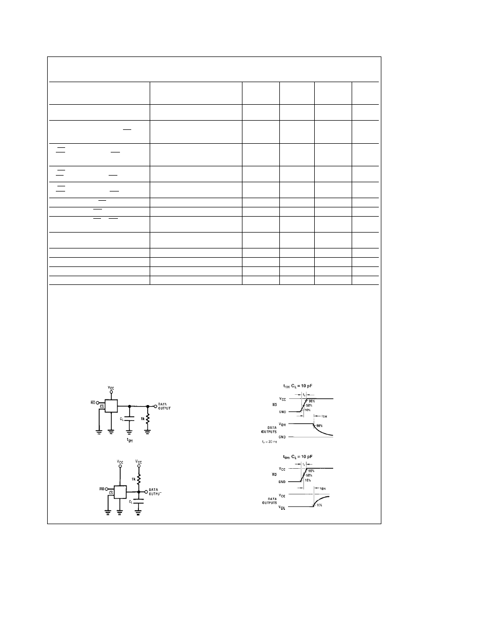
TRI-STATE Test Circuits and Waveforms
t
1H
TL H 5501 – 3
t
0H
TL H 5501 – 5
TL H 5501 – 4
t
r
e
20 ns
TL H 5501 – 6
4