Rainbow Electronics MAX4074_MAX4078 User Manual
Page 2
MAX4074–MAX4078
Micropower, SOT23, Rail-to-Rail,
Fixed-Gain, GainAmp/Open-Loop Op Amps
2
_______________________________________________________________________________________
ABSOLUTE MAXIMUM RATINGS
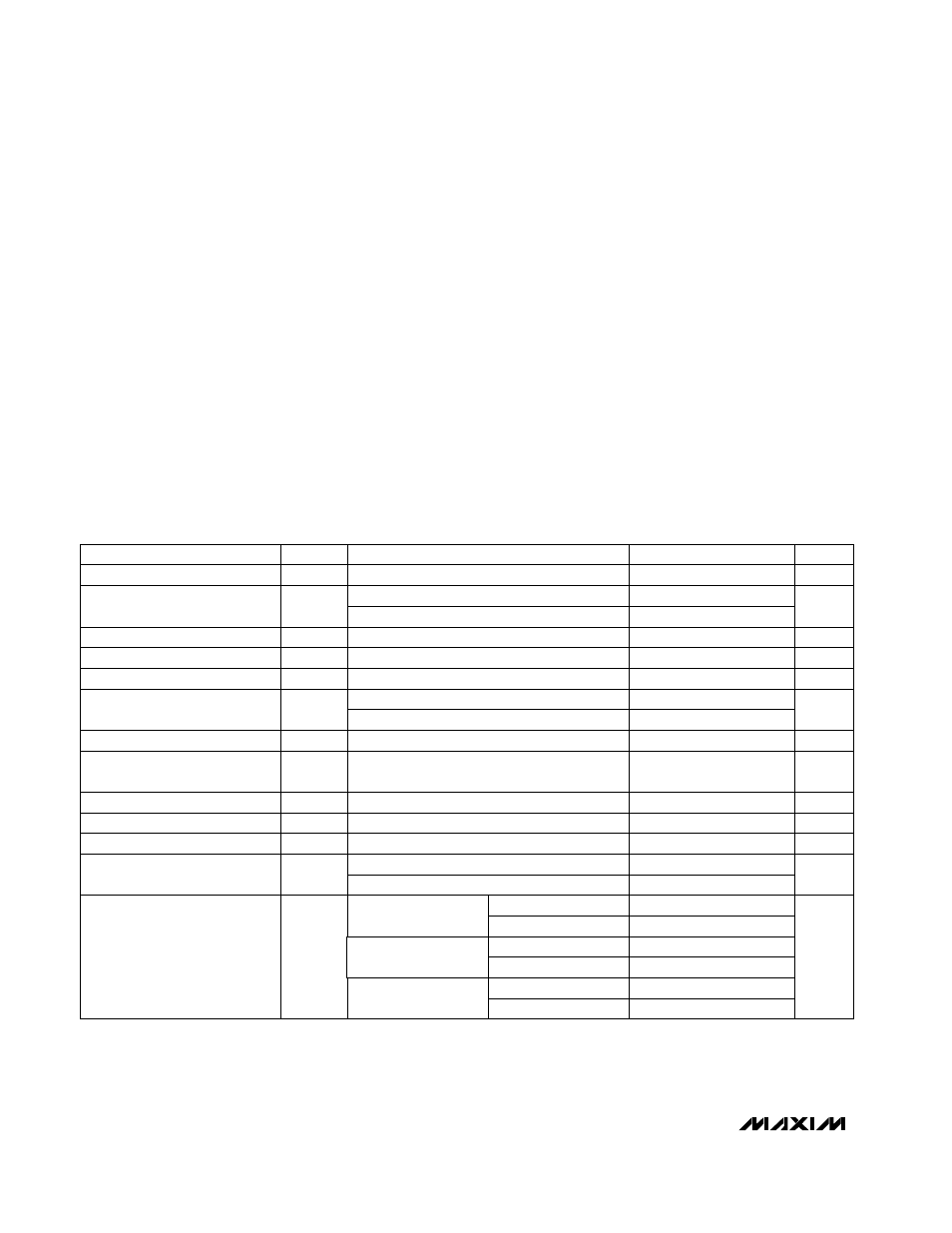
ELECTRICAL CHARACTERISTICS—MAX4074/MAX4075
(V
CC
= +2.5V to +5.5V, V
EE
= 0, V
IN+
= V
IN-
= V
CC
/2, R
L
=
∞
to V
CC
/2, T
A
= T
MIN
to T
MAX
, unless otherwise noted. Typical values
are at V
CC
= +5V and T
A
= +25°C.) (Note 1)
Stresses beyond those listed under “Absolute Maximum Ratings” may cause permanent damage to the device. These are stress ratings only, and functional
operation of the device at these or any other conditions beyond those indicated in the operational sections of the specifications is not implied. Exposure to
absolute maximum rating conditions for extended periods may affect device reliability.
Supply Voltages (V
CC
to V
EE
) ..................................-0.3V to +6V
Voltage Inputs (IN_)
MAX4076/MAX4077/MAX4078 .....(V
CC
+ 0.3V) to (V
EE
- 0.3V)
MAX4074/MAX4075..........................................................±17V
Output Short-Circuit Duration to Either Supply (OUT_). . . . Continuous
Continuous Power Dissipation (T
A
= +70°C)
5-Pin SOT23 (derate 7.1mW/°C above +70°C) ............571mW
14-Pin TSSOP (derate 6.3mW/°C above +70°C) ..........500mW
8-Pin µMAX (derate 4.1mW/°C above +70°C) ..............330mW
8-Pin SO (derate 5.88mW/°C above +70°C).................471mW
14-Pin SO (derate 8.33mW/°C above +70°C)...............667mW
Operating Temperature Range ...........................-40°C to +85°C
Junction Temperature ......................................................+150°C
Storage Temperature Range .............................-65°C to +150°C
Lead Temperature (soldering, 10sec) .............................+300°C
Supply Current (per amplifier)
I
CC
34
50
µA
V
CC
= 3V
PARAMETER
SYMBOL
MIN
TYP
MAX
UNITS
Inverting Input Resistance
R
IN_
80
k
Ω
V
CC
- V
OH
300
Input Bias Current (Note 2)
I
IN+_
0.8
1000
pA
Input Offset Voltage Drift
0.3
µV/°C
Noninverting Input Resistance
R
IN_+
1000
M
Ω
Negative Input Voltage Range
IN_-
±15
V
Power-Supply Rejection Ratio
PSRR
70
96
dB
Supply Voltage Range
V
CC
2.5
5.5
V
300
1000
37
55
Input Offset Voltage
V
OS
0.2
3.5
mV
Closed-Loop Output Impedance
R
OUT
0.2
Ω
V
CC
- V
OH
5
Output Short-Circuit Current
-22
mA
0.5
2.5
V
OL
- V
EE
Output Voltage Swing (Note 4)
100
600
mV
R
L
= 1k
Ω
V
CC
- V
OH
25
150
V
OL
- V
EE
Positive Input Voltage Range
IN_+
11
80
R
L
= 10k
Ω
V
OL
- V
EE
CONDITIONS
A
V
≥ +25V/V
Shorted to V
CC
A
V
< +25V/V
Shorted to V
EE
V
EE
-
V
CC
-
0.15
1.2
Guaranteed by functional test (Note 3)
V
CC
= 2.5V to 5.5V
V
Guaranteed by functional test (Note 3)
0.4
2.5
Guaranteed by PSRR test
V
CC
= 5V
R
L
= 1M
Ω
R
L
= 1M
Ω