Applications information – Rainbow Electronics MAX9758 User Manual
Page 21

Shutdown (
SHDN
)
The MAX9756/MAX9757/MAX9758 feature a 0.2µA,
low-power shutdown mode that reduces quiescent cur-
rent consumption and extends battery life. Driving
SHDN low disables the drive amplifiers, bias circuitry,
and charge pump, and drives BIAS and all outputs to
GND. Connect
SHDN to V
DD
for normal operation.
Click-and-Pop Suppression
Speaker Amplifier
The MAX9756/MAX9757/MAX9758 speaker amplifiers
feature Maxim’s comprehensive, industry-leading click-
and-pop suppression. During startup, the click-and-
pop suppression circuitry eliminates any audible
transient sources internal to the device. When entering
shutdown, both amplifier outputs ramp to GND quickly
and simultaneously.
Headphone Amplifier
In conventional single-supply headphone amplifiers, the
output-coupling capacitor is a major contributor of audi-
ble clicks and pops. Since the MAX9756/MAX9757/
MAX9758 do not require output-coupling capacitors, no
audible transient occurs.
Additionally, the MAX9756/MAX9757/MAX9758 feature
extensive click-and-pop suppression that eliminates any
audible transient sources internal to the device. The
Turn-On/Turn-Off waveforms in the Typical Operating
Characteristics show that there are minimal spectral
components in the audible range at the output upon
startup and shutdown.
Applications Information
BTL Speaker Amplifiers
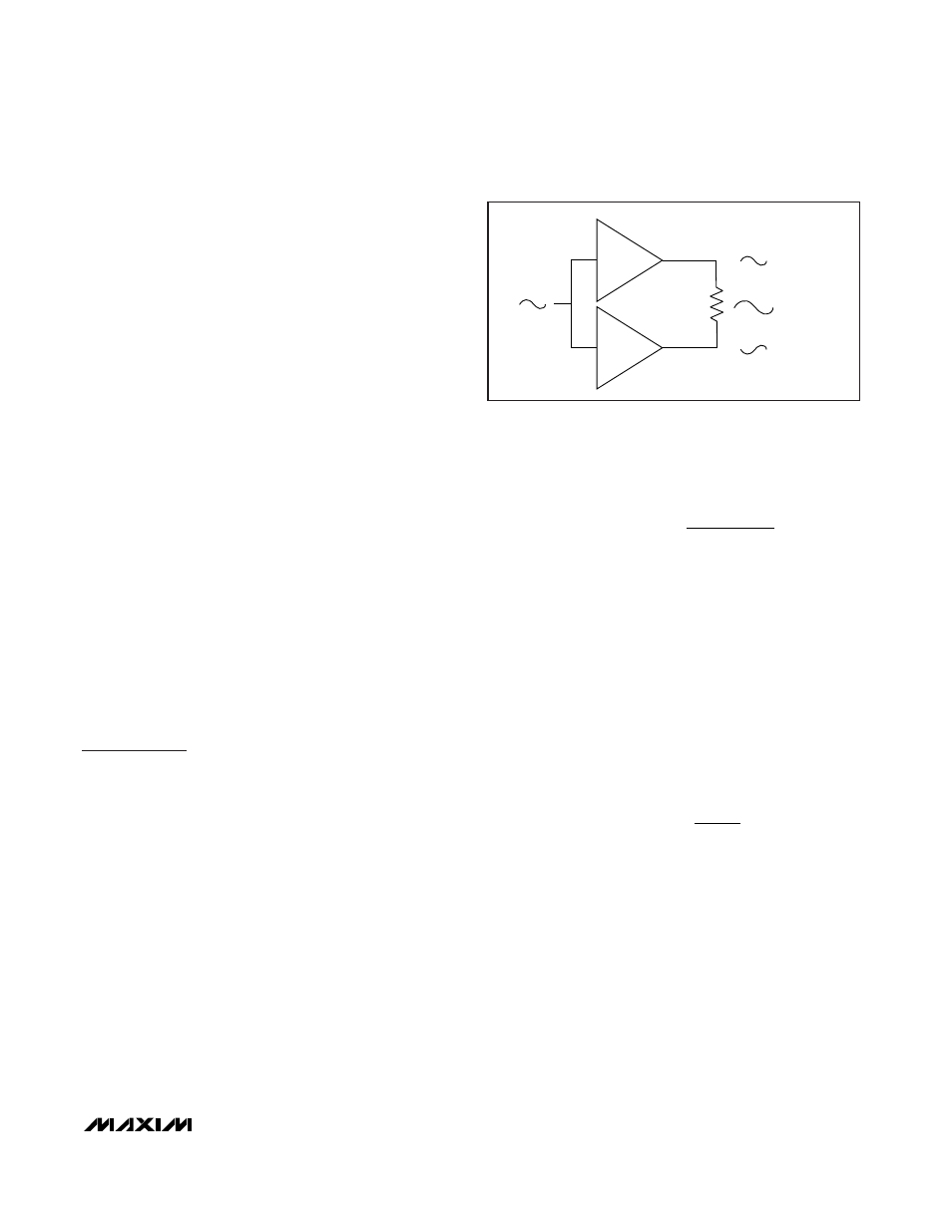
The MAX9756/MAX9757/MAX9758 feature speaker
amplifiers designed to drive a load differentially, a config-
uration referred to as bridge-tied load (BTL). The BTL
configuration (Figure 13) offers advantages over the sin-
gle-ended configuration, where one side of the load is
connected to ground. Driving the load differentially dou-
bles the output voltage compared to a single-ended
amplifier under similar conditions.
Since the differential outputs are biased at 2.5V, there is
no net DC voltage across the load. This eliminates the
need for DC-blocking capacitors required for single-
ended amplifiers. These capacitors can be large and
expensive, can consume board space, and can degrade
low-frequency performance.
Power Dissipation and Heat Sinking
Under normal operating conditions, the MAX9756/
MAX9757/MAX9758 can dissipate a significant amount
of power. The maximum power dissipation for each
package is given in the Absolute Maximum Ratings
under Continuous Power Dissipation, or can be calcu-
lated by the following equation:
where T
J(MAX)
is +150°C, T
A
is the ambient temperature,
and
θ
JA
is the reciprocal of the derating factor in °C/W as
specified in the Absolute Maximum Ratings section. For
example,
θ
JA
of the 32-pin thin QFN package is
+40.2°C/W. For optimum power dissipation, the exposed
paddle of the package should be connected to the
ground plane (see the Layout and Grounding section).
Output Power (Speaker Amplifier)
The increase in power delivered by the BTL configura-
tion directly results in an increase in internal power dis-
sipation over the single-ended configuration. The
maximum power dissipation for a given V
DD
and load is
given by the following equation:
If the power dissipation for a given application exceeds
the maximum allowed for a given package, either reduce
V
DD
, increase load impedance, decrease the ambient
temperature, or add heatsinking to the device or setting
PREF to limit output power to a safe level. Large output,
supply, and ground PC board traces improve the maxi-
mum power dissipation in the package. Thermal-over-
load protection limits total power dissipation in these
devices. When the junction temperature exceeds
+160°C, the thermal-protection circuitry disables the
amplifier output stage. The amplifiers are enabled once
the junction temperature cools by 15°C. This results in a
pulsing output under continuous thermal-overload condi-
tions as the device heats and cools.
P
V
R
DISS MAX
DD
L
(
)
=
2
2
2
π
P
T
DISSPKG MAX
J MAX
TA
JA
(
)
(
)
=
−
θ
MAX9756/MAX9757/MAX9758
2.3W Stereo Speaker Amplifiers and DirectDrive
Headphone Amplifiers with Automatic Level Control
______________________________________________________________________________________
21
Figure 13. Bridge-Tied Load Configuration
+1
V
OUT(P-P)
2 x V
OUT(P-P)
V
OUT(P-P)
-1
