Chip information, Pin configuration package information – Rainbow Electronics MAX15040 User Manual
Page 14

MAX15040
High-Efficiency, 4A, Step-Down Regulator with
Integrated Switches in 2mm x 2mm Package
14
______________________________________________________________________________________
PCB Layout Considerations and
Thermal Performance
Careful PCB layout is critical to achieve clean and stable
operation. It is highly recommended to duplicate the
MAX15040 evaluation kit layout for optimum performance.
If deviation is necessary, follow these guidelines for good
PCB layout:
1) Connect input and output capacitors to the power
ground plane; connect all other capacitors to the sig-
nal ground plane.
2) Place capacitors on V
DD
, IN, and REFIN/SS as close
as possible to the device and the corresponding
bump using direct traces. Keep power ground plane
and signal ground plane separate.
3) Keep the high-current paths as short and wide as
possible. Keep the path of switching current short
and minimize the loop area formed by LX, the out-
put capacitors, and the input capacitors.
4) Connect IN, LX, and GND separately to a large
copper area to help cool the device to further
improve efficiency and long-term reliability.
5) Ensure all feedback connections are short. Place
the feedback resistors and compensation compo-
nents as close to the device as possible.
6) Route high-speed switching nodes, such as LX and
BST, away from sensitive analog areas (FB, COMP).
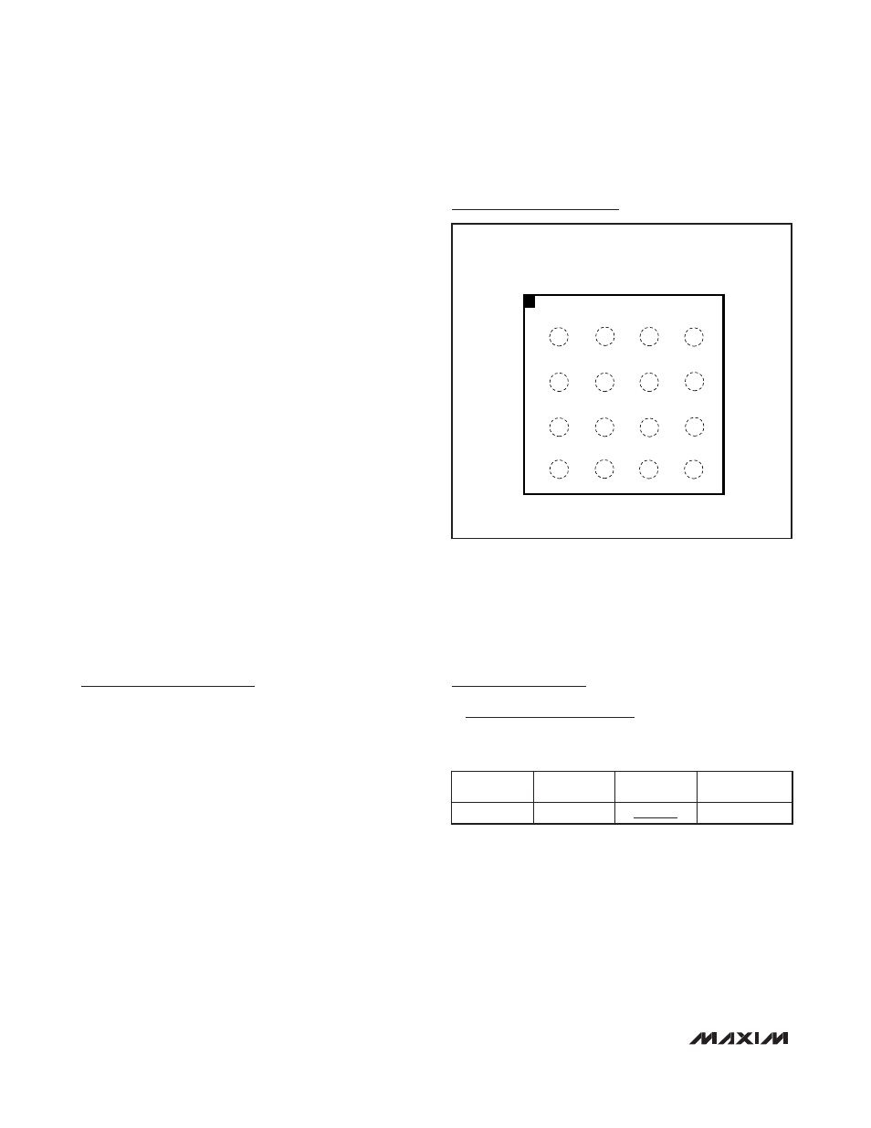
Chip Information
PROCESS: BiCMOS
WLP
GND
IN
IN
GND
A1
A2
A3
A4
B1
B2
B3
B4
C1
C2
C3
C4
D1
D2
D3
D4
LX
LX
V
DD
LX
I.C.
I.C.
EN
BST
PWRGD
FB
COMP
REFIN/SS
(BUMPS ON BOTTOM)
TOP VIEW
Pin Configuration
Package Information
For the latest package outline information and land patterns, go
. Note that a “+”, “#”, or “-” in
the package code indicates RoHS status only. Package draw-
ings may show a different suffix character, but the drawing per-
tains to the package regardless of RoHS status.
PACKAGE
TYPE
PACKAGE
CODE
OUTLINE
NO.
LAND
PATTERN NO.
16 WLP
W162B2+1
—
