Rainbow Electronics MAX15040 User Manual
Page 13
MAX15040
The zero-cross frequency of the closed-loop, f
C
, should
be between 10% and 20% of the switching frequency,
f
S
(1MHz). A higher zero-cross frequency results in
faster transient response. Once f
C
is chosen, C1 is cal-
culated from the following equation:
where V
P-P
= 1V
P-P
(typ).
Due to the underdamped nature of the output LC dou-
ble pole, set the two zero frequencies of the type III
compensation less than the LC double-pole frequency
to provide adequate phase boost. Set the two zero fre-
quencies to 80% of the LC double-pole frequency.
Hence:
Setting the second compensation pole, f
P2_EA
, at
f
Z_ESR
yields:
Set the third compensation pole at 1/2 of the switching
frequency (500kHz) to gain phase margin. Calculate
C2 as follows:
The above equations provide accurate compensation
when the zero-cross frequency is significantly higher than
the double-pole frequency. When the zero-cross frequen-
cy is near the double-pole frequency, the actual zero-
cross frequency is higher than the calculated frequency.
In this case, lowering the value of R1 reduces the zero-
cross frequency. Also, set the third pole of the type III
compensation close to the switching frequency (1MHz) if
the zero-cross frequency is above 200kHz to boost the
phase margin. The recommended range for R3 is 2k
Ω to
10k
Ω. Note that the loop compensation remains
unchanged if only R4’s resistance is altered to set differ-
ent outputs.
Soft-Starting into a Prebiased Output
The MAX15040 soft-starts into a prebiased output without
discharging the output capacitor. In safe prebiased start-
up, both low-side and high-side switches remain off to
avoid discharging the prebiased output. PWM operation
starts when the voltage on REFIN/SS crosses the voltage
on FB. The PWM activity starts with the low-side switch
turning on first to build the bootstrap capacitor charge.
Power-good (PWRGD) asserts 48 clock cycles after FB
crosses 92.5% of the final regulation set point. After 4096
clock cycles, the device switches from prebiased safe
startup mode to forced PWM mode.
The MAX15040 is capable of starting into a prebias volt-
age higher than the nominal set point without abruptly dis-
charging the output. This is achieved by using the sink
current control of the low-side MOSFET, which has four
internally set sinking current-limit thresholds. An internal
4-bit DAC steps through these thresholds, starting from
the lowest current limit to the highest, in 128 clock cycles
on every power-up.
C
x R x f
S
2
1
1
=
π
R
C
x ESR
C
O
2
3
=
C
x R
x
L x C
x R
ESR
R
R
O
O
L
O
3
1
0 8
3
=
+
+
.
(
)
R
x C
x
L x C
x R
ESR
R
R
O
O
L
O
1
1
0 8
1
=
+
+
.
(
)
C
V
V
x
x R x
R
R
f
IN
P P
L
O
C
1
2 5
2
3
1
=
⎛
⎝⎜
⎞
⎠⎟
+
×
−
.
(
)
π
High-Efficiency, 4A, Step-Down Regulator with
Integrated Switches in 2mm x 2mm Package
______________________________________________________________________________________
13
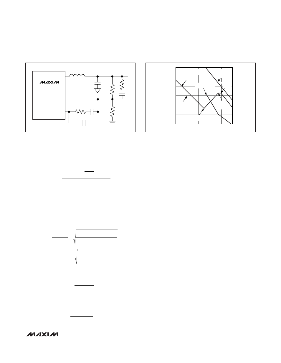
L
C
OUT
V
OUT
R3
R4
R1
COMP
FB
LX
C1
C3
R2
C2
MAX15040
Figure 4. Type III Compensation Network
DOUBLE POLE
GAIN (dB)
FREQUENCY (Hz)
SECOND
POLE
FIRST AND SECOND ZEROS
POWER-STAGE
TRANSFER
FUNCTION
COMPENSATION
TRANSFER
FUNCTION
OPEN-LOOP
GAIN
THIRD
POLE
Figure 5. Type III Compensation Illustration