Rainbow Electronics MAX15040 User Manual
Page 12

MAX15040
High-Efficiency, 4A, Step-Down Regulator with
Integrated Switches in 2mm x 2mm Package
Input-Capacitor Selection
The input capacitor reduces the current peaks drawn
from the input power supply and reduces switching
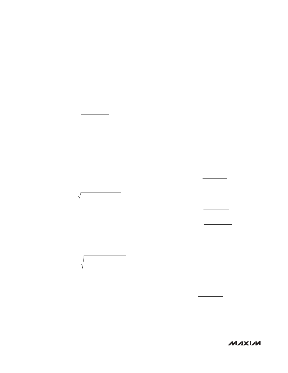
noise in the device. The total input capacitance must
be equal to or greater than the value given by the fol-
lowing equation to keep the input ripple voltage within
the specification and minimize the high-frequency rip-
ple current being fed back to the input source:
where V
IN-RIPPLE
is the maximum allowed input ripple
voltage across the input capacitors and is recommend-
ed to be less than 2% of the minimum input voltage, D
is the duty cycle (V
OUT
/V
IN
), and T
S
is the switching
period (1/f
S
) = 1µs.
The impedance of the input capacitor at the switching
frequency should be less than that of the input source so
high-frequency switching currents do not pass through
the input source, but are instead shunted through the
input capacitor. The input capacitor must meet the ripple
current requirement imposed by the switching currents.
The RMS input ripple current is given by:
where I
RIPPLE
is the input RMS ripple current.
Compensation Design
The power transfer function consists of one double pole
and one zero. The double pole is introduced by the
inductor, L, and the output capacitor, C
O
. The ESR of the
output capacitor determines the zero. The double pole
and zero frequencies are given as follows:
where R
L
is equal to the sum of the output inductor’s DC
resistance (DCR) and the internal switch resistance,
R
DSON
. A typical value for R
DSON
is 15m
Ω. R
O
is the
output load resistance, which is equal to the rated output
voltage divided by the rated output current. ESR is the
total equivalent series resistance of the output capacitor.
If there is more than one output capacitor of the same
type in parallel, the value of the ESR in the above equa-
tion is equal to that of the ESR of a single output capaci-
tor divided by the total number of output capacitors.
The MAX15040 high switching frequency allows the use
of ceramic output capacitors. Since the ESR of ceramic
capacitors is typically very low, the frequency of the
associated transfer function zero is higher than the unity-
gain crossover frequency, f
C
, and the zero cannot be
used to compensate for the double pole created by the
output inductor and capacitor. The double pole produces
a gain drop of 40dB/decade and a phase shift of 180°.
The compensation network must compensate for this
gain drop and phase shift to achieve a stable high-band-
width closed-loop system. Therefore, use type III com-
pensation as shown in Figure 4 and Figure 5. Type III
compensation possesses three poles and two zeros with
the first pole, f
P1_EA
, located at zero frequency (DC).
Locations of other poles and zeros of the type III compen-
sation are given by:
The above equations are based on the assumptions that
C1 >> C2, and R3 >> R2, which are true in most appli-
cations. Placements of these poles and zeros are deter-
mined by the frequencies of the double pole and ESR
zero of the power transfer function. It is also a function
of the desired closed-loop bandwidth. The following
section outlines the step-by-step design procedure to
calculate the required compensation components for
the MAX15040.
The output voltage is determined by:
For V
OUT
= 0.6V, R4 is not needed.
R
R
V
OUT
4
0 6
3
0 6
=
×
−
(
)
.
.
f
x R
x C
P
EA
1
2
2
3
2 _
=
π
f
x
P
EA
3
1
2
_
=
π R
R x C
1
2
f
x R x C
Z
EA
2
1
2
3
3
_
=
π
f
x R x C
Z
EA
1
1
2
1
1
_
=
π
f
x ESR x C
Z ESR
O
_
=
1
2
π
f
f
x L x C
x
R
ESR
R
R
P
LC
P
LC
O
O
O
L
1
2
1
2
_
_
=
=
+
+
⎛
⎝⎜
⎞
⎠⎟
π
I
I
V
V
V
V
RIPPLE
LOAD
OUT
IN
OUT
IN
=
Ч
Ч
−
(
)
C
D x T x I
V
IN MIN
S
OUT
IN RIPPLE
_
=
−
12
______________________________________________________________________________________
