Detailed description, Table 1. unipolar code current – Rainbow Electronics MAX5362 User Manual
Page 8
MAX5360/MAX5361/MAX5362
Low-Cost, Low-Power 6-Bit DACs with
2-Wire Serial Interface in SOT23 Package
8
_______________________________________________________________________________________
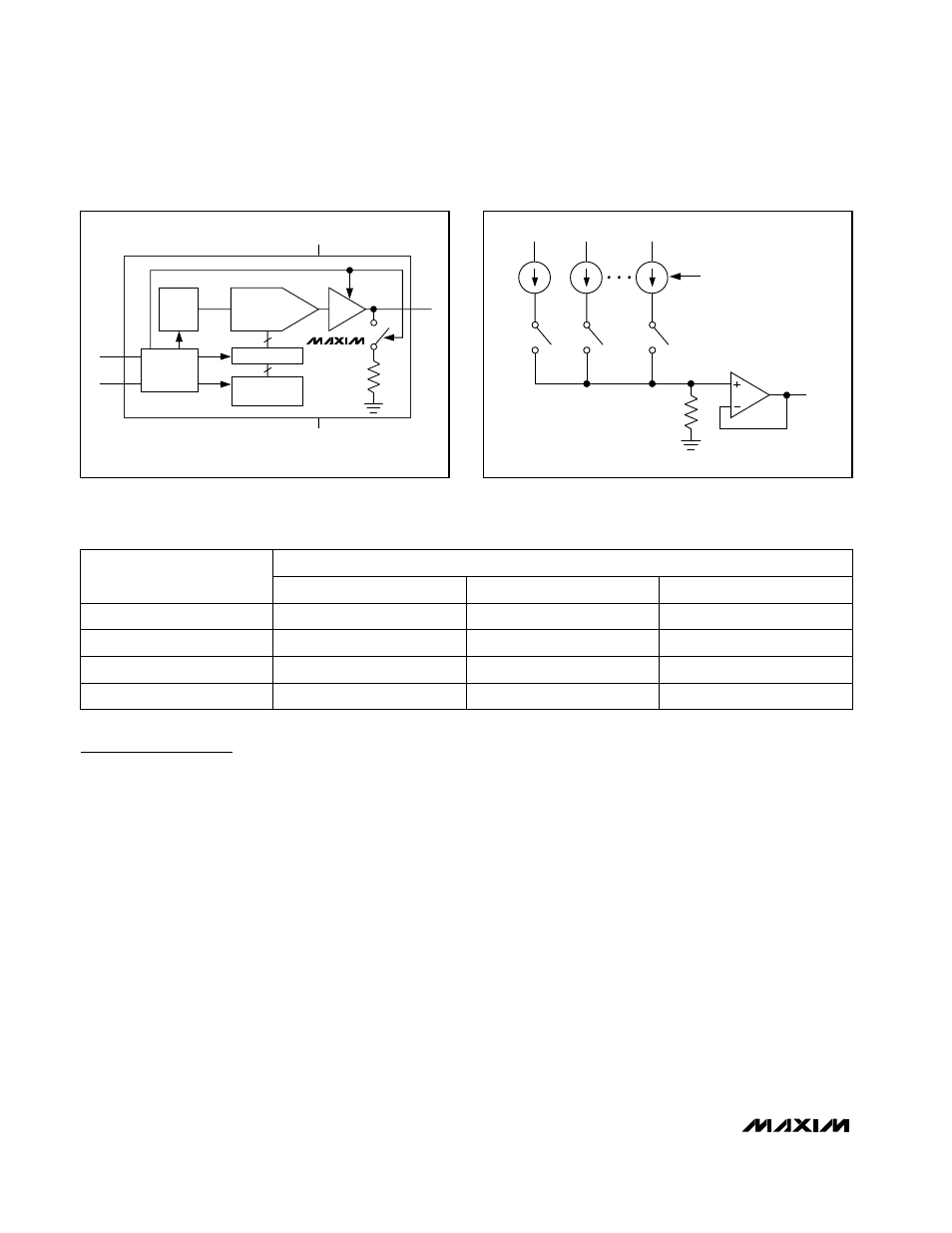
Detailed Description
The MAX5360/MAX5361/MAX5362 voltage-output, 6-bit
DACs offer full 6-bit performance with less than 1LSB
integral nonlinearity (INL) error and less than 1LSB dif-
ferential nonlinearity (DNL) error ensuring monotonic
performance. The devices use a simple two-wire, fast-
mode I
2
C-compatible serial interface that operates up
to 400kHz. The MAX5360/MAX5361/MAX5362 include
an internal reference, an output buffer, and low-current
shutdown mode, making them ideal for low-power,
highly integrated applications. Figure 1 shows the
devices’ functional diagram.
Analog Section
The MAX5360/MAX5361/MAX5362 employ a current-
steering DAC topology as shown in Figure 2. At the
core of the DAC is a reference voltage-to-current con-
verter (V/I) that generates a reference current. This cur-
rent is mirrored to 255 equally weighted current
sources. DAC switches control the outputs of these cur-
rent mirrors, so only the desired fraction of the total cur-
rent-mirror currents is steered to the DAC output. The
current is then converted to a voltage across a resistor,
and this voltage is buffered by the output buffer amplifier.
Output Voltage
Table 1 shows the relationship between the DAC code
and the analog output voltage. The 6-bit DAC code is
binary unipolar with 1LSB = (V
REF
/ 64). The MAX5360/
MAX5361 have a full-scale output voltage of (+2V -
1LSB) and (+4V - 1LSB), respectively, set by the inter-
nal references. The MAX5362 has a full-scale output
voltage of (0.9
✕
V
DD
- 1LSB). Each device accepts 8-bit
DAC codes, but the accuracy is guaranteed only for
6 bits.
Output Buffer
The DAC voltage output is an internally buffered unity-
gain follower that typically slews at ±0.4V/µs. The out-
put can swing from 0 to full scale. With a 1/4 FS to 3/4
FS output transition, the amplifier outputs typically settle
to 1/2LSB in less than 5µs when loaded with 10k
Ω in
parallel with 50pF. The buffer amplifiers are stable with
any combination of resistive loads >10k
Ω and capaci-
tive loads <50pF.
V
REF
OUT
SW1
SW2
SW255
Figure 2. Current-Steering Topology
V
DD
OUT
10k
GND
SDA
SCL
255
6 + 2
CURRENT-
STEERING
DAC
DATA LATCH
SERIAL INPUT
REGISTER
CONTROL
LOGIC
MAX5360
MAX5361
MAX5362
REF
Figure 1. Functional Diagram
Table 1. Unipolar Code Current
000001 (00)
0.9
✕
V
DD
/ 64
62mV
31mV
000000 (00)
0
0
0
100000 (00)
0.9
✕
V
DD
/ 2
2V
1V
111111 (00)
0.9
✕
V
DD ✕
(63/64)
4V
✕
(63/64)
2V
✕
(63/64)
MAX5362
MAX5361
MAX5360
DAC CODE
6 BITS + 2 SUBBITS
OUTPUT VOLTAGE