Vishay semiconductors – C&H Technology VS-175BGQ030 User Manual
Page 5
VS-175BGQ030
www.vishay.com
Vishay Semiconductors
Revision: 04-Jul-11
4
Document Number: 94583
For technical questions within your region:
,
,
THIS DOCUMENT IS SUBJECT TO CHANGE WITHOUT NOTICE. THE PRODUCTS DESCRIBED HEREIN AND THIS DOCUMENT
ARE SUBJECT TO SPECIFIC DISCLAIMERS, SET FORTH AT
www.vishay.com/doc?91000
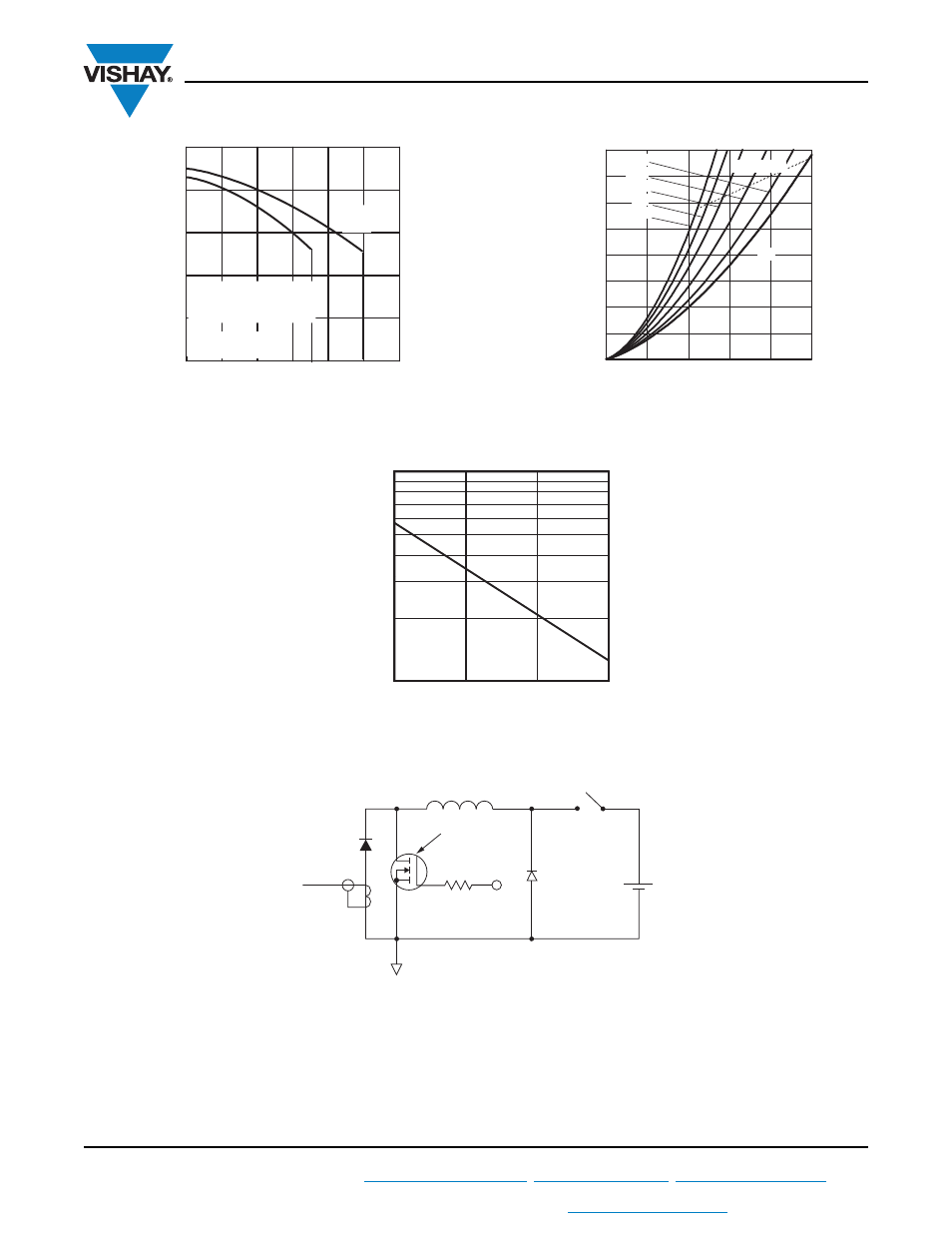
Fig. 5 - Maximum Allowable Case Temperature vs.
Average Forward Current
Fig. 6 - Forward Power Loss Characteristics
Fig. 7 - Maximum Non-Repetitive Surge Current
Fig. 8 - Unclamped Inductive Test Circuit
Note
(1)
Formula used: T
C
= T
J
- (Pd + Pd
REV
) x R
thJC
;
Pd = Forward power loss = I
F(AV)
x V
FM
at (I
F(AV)
/D) (see fig. 6);
Pd
REV
= Inverse power loss = V
R1
x I
R
(1 - D); I
R
at V
R1
= 80 % rated V
R
Average Forward Current - I
F
(AV)
(A)
Allowable Case Temperature (°C)
0
50
100
150
200
250
300
60
80
100
120
140
160
DC
Square wave (D=0.50)
80% rated Vr applied
see note (1)
Average Forward Current - I
F
(AV)
(A)
Average Power Loss - (Watts)
0
50
100
150
200
250
0
20
40
60
80
100
120
140
160
180°
120°
90°
60°
30°
DC
RMS Limit
Square Wave Pulse Duration - t
p
(microsec)
Non-Repetitive Surge Current - I
FSM
(A)
10
100
1000
10000
1000
10000
Current
monitor
High-speed
switch
D.U.T.
R
g
= 25
Ω
+
Freewheel
diode
V
d
= 25 V
L
IRFP460
40HFL40S02