Cpv362m4fpbf, Vishay high power products, Igbt sip module (fast igbt) – C&H Technology CPV362M4FPbF User Manual
Page 3: Electrical characteristics (t, 25 °c unless otherwise specified), Switching characteristics (t
www.vishay.com
For technical questions, contact: [email protected]
Document Number: 94361
2
Revision: 29-Apr-08
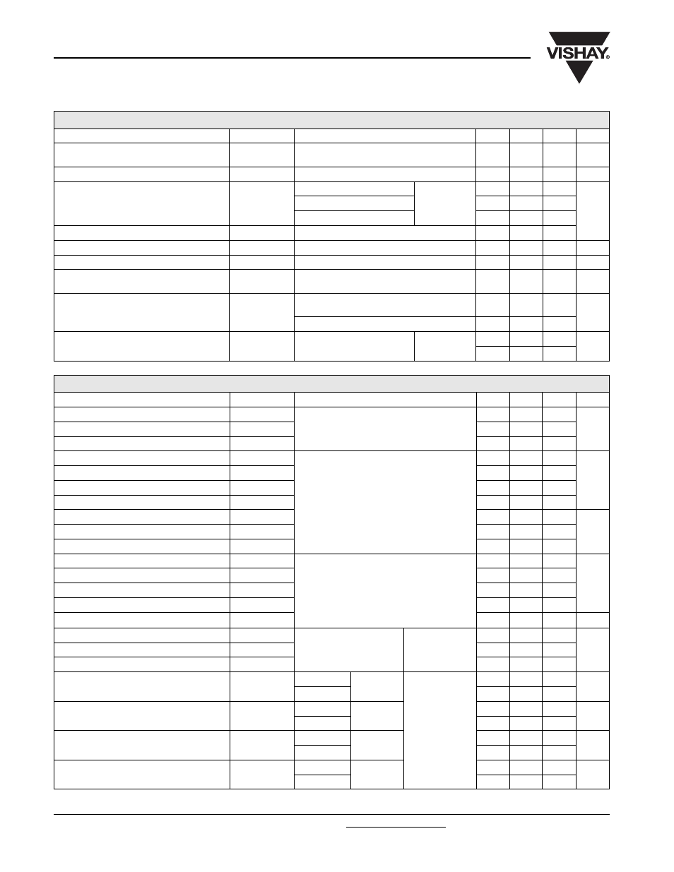
CPV362M4FPbF
Vishay High Power Products
IGBT SIP Module
(Fast IGBT)
ELECTRICAL CHARACTERISTICS (T
J
= 25 °C unless otherwise specified)
PARAMETER SYMBOL
TEST
CONDITIONS
MIN.
TYP.
MAX.
UNITS
Collector to emitter breakdown voltage
V
(BR)CES
V
GE
= 0 V, I
C
= 250 µA
Pulse width
≤ 80 µs, duty factor ≤ 0.1 %
600
-
-
V
Temperature coeff. of breakdown voltage
ΔV
(BR)CES
/ΔT
J
V
GE
= 0 V, I
C
= 1.0 mA
-
0.72
-
V/°C
Collector to emitter saturation voltage
V
CE(on)
I
C
= 4.8 A
V
GE
= 15 V
See fig. 2, 5
-
1.41
1.7
V
I
C
= 8.8 A
-
1.66
-
I
C
= 4.8 A, T
J
= 150 °C
-
1.42
-
Gate threshold voltage
V
GE(th)
V
CE
= V
GE
, I
C
= 250 µA
3.0
-
6.0
Gate to emitter leakage current
I
GES
V
GE
= ± 20 V
-
-
± 100
nA
Temperature coeff. of threshold voltage
ΔV
GE(th)
/
ΔT
J
V
GE
= 0 V, I
C
= 1.0 mA
-
-11
-
mV/°C
Forward transconductance
g
fe
V
CE
= 100 V, I
C
= 4.8 A
Pulse width 5.0 µs; single shot
2.9
5.0
-
S
Zero gate voltage collector current
I
CES
V
GE
= 0 V, V
CE
= 600 V
-
-
250
µA
V
GE
= 0 V, V
CE
= 600 V, T
J
= 150 °C
-
-
1700
Diode forward voltage drop
V
FM
I
C
= 8.0 A
I
C
= 8.0 A, T
J
= 150 °C
See fig. 13
-
1.4
1.7
V
-
1.3
1.6
SWITCHING CHARACTERISTICS (T
J
= 25 °C unless otherwise specified)
PARAMETER SYMBOL
TEST
CONDITIONS
MIN.
TYP.
MAX.
UNITS
Total gate charge (turn on)
Q
g
I
C
= 4.8 A
V
CC
= 400 V
See fig. 8
-
30
45
nC
Gate to emitter charge (turn on)
Q
ge
-
4.0
6.0
Gate to collector charge
Q
gc
-
13
20
Turn-on delay time
t
d(on)
T
J
= 25 °C
I
C
= 4.8 A, V
CC
= 480 V
V
GE
= 15 V, R
G
= 50
Ω
Energy losses include “tail” and diode
reversev recovery.
See fig. 9, 10, 18
-
49
-
ns
Rise time
t
r
-
22
-
Turn-off delay time
t
d(off)
-
200
300
Fall time
t
f
-
214
320
Turn-on switching loss
E
on
-
0.23
-
mJ
Turn-off switching loss
E
off
-
0.33
-
Total switching loss
E
ts
-
0.45
0.70
Turn-on delay time
t
d(on)
T
J
= 150 °C,
I
C
= 4.8 A, V
CC
= 480 V
V
GE
= 15 V, R
G
= 50
Ω
Energy losses include “tail” and
diode reverse recovery
See fig. 10, 11, 18
-
48
-
ns
Rise time
t
r
-
25
-
Turn-off delay time
t
d(off)
-
435
-
Fall time
t
f
-
364
-
Total switching loss
E
ts
-
0.93
-
mJ
Input capacitance
C
ies
V
GE
= 0 V
V
CC
= 30 V
See fig. 7
-
340
-
pF
Output capacitance
C
oes
-
63
-
Reverse transfer capacitance
C
res
-
5.9
-
Diode reverse recovery time
t
rr
T
J
= 25 °C
See fig. 14
I
F
= 8.0 A
V
R
= 200 V
dI/dt = 200 A/µs
-
37
55
ns
T
J
= 125 °C
-
55
90
Diode peak reverse recovery current
I
rr
T
J
= 25 °C
See fig. 15
-
3.5
50
A
T
J
= 125 °C
-
4.5
8.0
Diode reverse recovery charge
Q
rr
T
J
= 25 °C
See fig. 16
-
65
138
nC
T
J
= 125 °C
-
124
360
Diode peak rate of fall of recovery during t
b
dI
(rec)M
/dt
T
J
= 25 °C
See fig. 17
-
240
-
A/µs
T
J
= 125 °C
-
210
-