Thermal resistance characteristics, Mechanical characteristics, Recommended operating conditons, ta = 25°c – C&H Technology CM600DU-12NFH User Manual
Page 5
CM600DU-12NFH
Dual IGBTMOD™ NFH-Series Module
600 Amperes/600 Volts
4
Powerex, Inc., 173 Pavilion Lane, Youngwood, Pennsylvania 15697 (724) 925-7272 www.pwrx.com
07/11 Rev. 2
Thermal Resistance Characteristics
Thermal Resistance, Junction to Case
*2
Rth(j-c)Q
Per IGBT
—
—
0.11
K/W
Thermal Resistance, Junction to Case
*2
Rth(j-c)D
Per FWDi
—
—
0.12
K/W
Contact Thermal Resistance,
Rth(c-f)
Thermal Grease Applied
—
0.02
— K/W
Case to Heatsink
*2
(Per 1 Module)
*7
Thermal Resistance, Junction to Case
*3
Rth(j-c')Q
Per IGBT
—
—
0.053
K/W
Thermal Resistance, Junction to Case
*3
Rth(j-c')D
Per FWDi
—
—
0.078
K/W
Mechanical Characteristics
Mounting Torque
Mt
Main Terminals, M6 Screw
31
35
40
in-lb
Ms
Mounting to Heatsink, M6 Screw
31 35 40 in-lb
Weight
m
— 580 — Grams
Flatness of Baseplate
ec
On Centerline X, Y
*8
-100 — +100 µm
Recommended Operating Conditons,
Ta = 25°C
(DC) Supply Voltage
VCC
Applied Across C1-E2
—
300
400
Volts
Gate (-Emitter Drive) Voltage
VGE(on)
Applied Across G1-Es1 / G2-Es2
13.5
15.0
16.5
Volts
External Gate Resistance
RG
Per Switch
1.0
—
10
Ω
*2 Case temperature (TC) and heatsink temperature (Ts) is measured on the surface
(mounting side) of the baseplate and the heatsink side just under the chips.
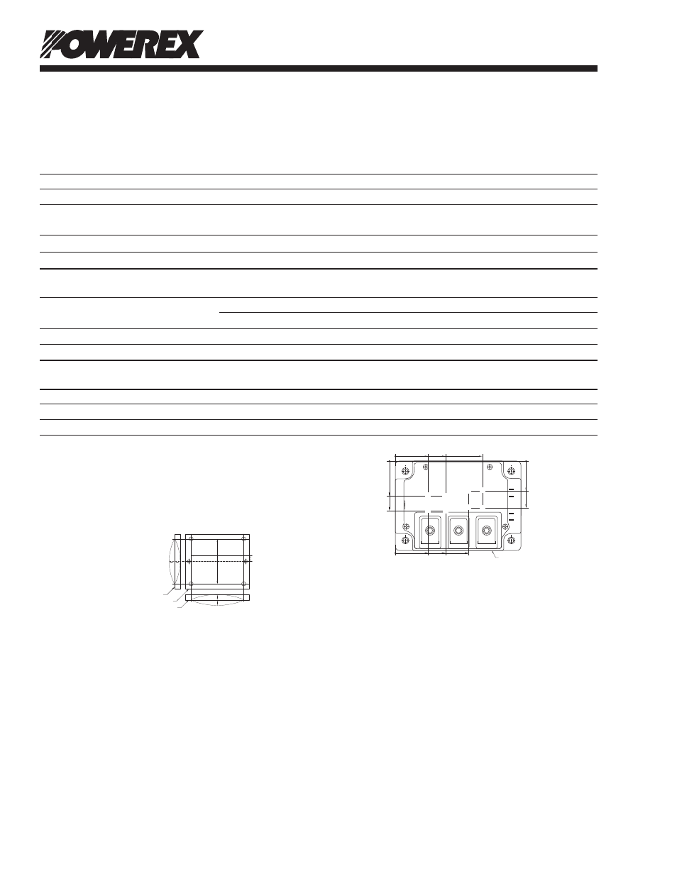
Refer to the figure to the right for chip location.
The heatsink thermal resistance should be measured just under the chips.
*3 Case temperature (TC') and heatsink temperature (Ts') is measured on the surface
(mounting side) of the baseplate and the heatsink side just under the chips.
Refer to the figure to the right for chip location.
The heatsink thermal resistance {Rth(s-a)} should be measured just under the chips.
*7 Typical value is measured by using thermally conductive grease of λ = 0.9 [W/(m • K)].
*8 Baseplate (mounting side) flatness measurement points (X, Y) are shown in the figure below.
0
29.4
44.2
77
.2
29.4
44.2
64.8
32.0
44.4
27.3
42.1
G2
E2
E1
G1
C2E1
C1
E2
0
0
0
LABEL SIDE
Each mark points to the center position of each chip.
Tr1 / Tr2 : IGBT Di1 / Di2 : FWDi
Di1
Di1
Tr1
Tr1
Di2
Di2
Tr2
Tr2
X
BOTTOM
– CONCAVE
3 mm
+ CONVEX
– CONCAVE
+ CONVEX
BOTTOM
BOTTOM
LABEL SIDE
Y