C&H Technology CM600DU-12NFH User Manual
Page 3
CM600DU-12NFH
Dual IGBTMOD™ NFH-Series Module
600 Amperes/600 Volts
2
Powerex, Inc., 173 Pavilion Lane, Youngwood, Pennsylvania 15697 (724) 925-7272 www.pwrx.com
07/11 Rev. 2
Absolute Maximum Ratings,
Tj = 25 °C unless otherwise specified
Item
Symbol Rating Units
Collector-Emitter Voltage (G-E Short-circuited)
VCES 600 Volts
Gate-Emitter Voltage (C-E Short-circuited)
VGES ±20 Volts
Collector Current (Operation)
*5
IC
600 Amperes
Collector Current (Operation)
*5
IC(rms) 400 Amperes
Collector Current (Pulse, Repetitive)
*4
ICRM 1200 Amperes
Total Power Dissipation (TC = 25°C)
*2,*5
Ptot 1130 Watts
Total Power Dissipation (TC' = 25°C)
*3,*5
Ptot' 2350 Watts
Emitter Current (Free Wheeling Diode Forward Current, Operation)
*5
IE
*1
600 Amperes
Emitter Current (Free Wheeling Diode Forward Current, Operation)
*5
IE(rms)
*1
400 Amperes
Emitter Current (Free Wheeling Diode Forward Current, Operation, Pulse, Repetitive)
*4
IERM
*1
1200 Amperes
Junction Temperature
Tj
–40 to 150
°C
Storage Temperature
Tstg
–40 to 125
°C
Isolation Voltage (Terminals to Baseplate, RMS, f = 60Hz, AC 1 min.)
VISO 2500 Volts
*1 Represent ratings and characteristics of the anti-parallel, emitter-to-collector free wheeling diode (FWDi).
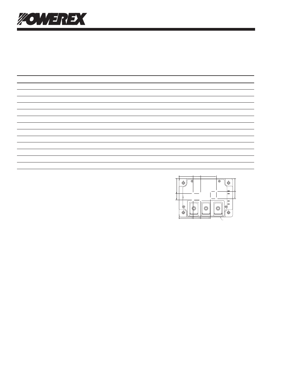
*2 Case temperature (TC) and heatsink temperature (Ts) is measured on the surface
(mounting side) of the baseplate and the heatsink side just under the chips.
Refer to the figure to the right for chip location.
*3 Case temperature (TC') and heatsink temperature (Ts') is measured on the surface
(mounting side) of the baseplate and the heatsink side just under the chips.
Refer to the figure to the right for chip location.
The heatsink thermal resistance {Rth(s-a)} should be measured just under the chips.
*4 Pulse width and repetition rate should be such that device junction temperature (Tj)
does not exceed Tj(max) rating.
*5 Junction temperature (Tj) should not increase beyond maximum junction
temperature (Tj(max)) rating.
0
29.4
44.2
77
.2
29.4
44.2
64.8
32.0
44.4
27.3
42.1
G2
E2
E1
G1
C2E1
C1
E2
0
0
0
LABEL SIDE
Each mark points to the center position of each chip.
Tr1 / Tr2 : IGBT Di1 / Di2 : FWDi
Di1
Di1
Tr1
Tr1
Di2
Di2
Tr2
Tr2