Vishay semiconductors – C&H Technology GA100TS120UPbF User Manual
Page 8
VS-GA100TS120UPbF
www.vishay.com
Vishay Semiconductors
Revision: 26-Mar-12
7
Document Number: 94428
For technical questions within your region:
,
,
THIS DOCUMENT IS SUBJECT TO CHANGE WITHOUT NOTICE. THE PRODUCTS DESCRIBED HEREIN AND THIS DOCUMENT
ARE SUBJECT TO SPECIFIC DISCLAIMERS, SET FORTH AT
www.vishay.com/doc?91000
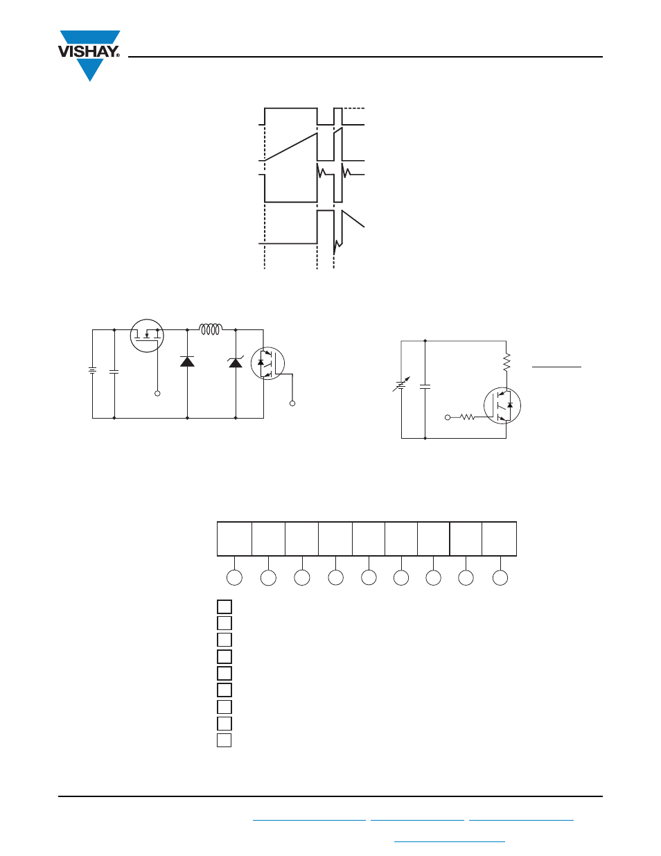
Fig. 17e - Macro Waveforms for Figure 18a‘s Test Circuit
Fig. 18 - Clamped Inductive Load Test Circuit
Fig. 19 - Pulsed Collector Current Test Circuit
ORDERING INFORMATION TABLE
V
G
Gate signal
device under test
Current D.U.T.
Voltage in D.U.T.
Current in D1
t0
t1
t2
D.U.T.
50 V
L
V
C
*
1000 V
6000 µF
100 V
* Driver same type as D.U.T.; V
C
= 80 % of V
CE
(max)
Note: Due to the 50 V power supply, pulse width and inductor
will increase to obtain rated I
d
480 V
4 x I
C
at 25 °C
0 - 480 V
R
L
=
=
2
-
Insulated gate bipolar transistor (IGBT)
1
-
Vishay Semiconductors product
3
-
Generation 4, IGBT silicon, DBC construction
4
-
Current rating (100 = 100 A)
5
-
Circuit configuration (T = Half-bridge)
6
-
Package indicator (INT-A-PAK)
7
-
Voltage rating (120 = 1200 V)
8
-
Speed/type (U = Ultrafast)
9
-
PbF = Lead (Pb)-free
Device code
5
1
3
2
4
6
7
8
9
G
VS-
A
100
T
S
120
U
PbF