Vishay semiconductors, Electrical specifications (t, 25 °c unless otherwise specified) – C&H Technology GA100TS120UPbF User Manual
Page 3: Switching characteristics (t
VS-GA100TS120UPbF
www.vishay.com
Vishay Semiconductors
Revision: 26-Mar-12
2
Document Number: 94428
For technical questions within your region:
,
,
THIS DOCUMENT IS SUBJECT TO CHANGE WITHOUT NOTICE. THE PRODUCTS DESCRIBED HEREIN AND THIS DOCUMENT
ARE SUBJECT TO SPECIFIC DISCLAIMERS, SET FORTH AT
www.vishay.com/doc?91000
Note
(1)
Repetitive rating; V
GE
= 20 V, pulse width limited by maximum junction temperature
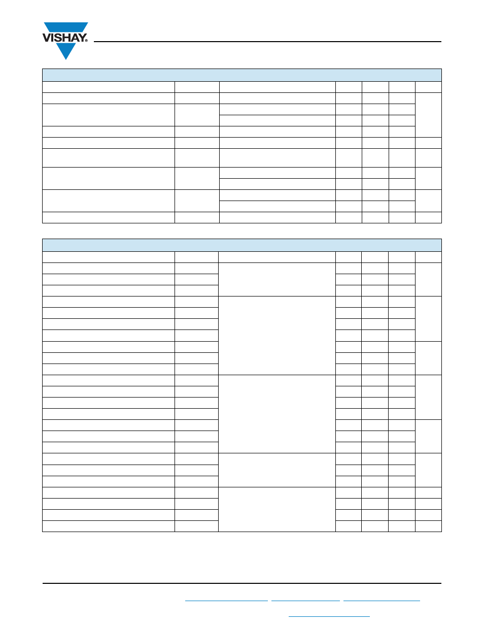
ELECTRICAL SPECIFICATIONS (T
J
= 25 °C unless otherwise specified)
PARAMETER SYMBOL
TEST
CONDITIONS MIN.
TYP.
MAX.
UNITS
Collector to emitter breakdown voltage
V
(BR)CES
V
GE
= 0 V, I
C
= 1 mA
1200
-
-
V
Collector to emitter voltage
V
CE(on)
V
GE
= 15 V, I
C
= 100 A
-
2.25
3
V
GE
= 15 V, I
C
= 100 A, T
J
= 125 °C
-
2
2.4
Gate threshold voltage
V
GE(th)
I
C
= 1.25 mA
3.0
4.4
6.0
Temperature coefficient of threshold voltage
V
GE(th)
/
T
J
V
CE
= V
GE
, I
C
= 1.25 mA
-
- 12
-
mV/°C
Forward transconductance
g
fe
V
CE
= 25 V, I
C
= 100 A
Pulse width 50 μs, single shot
-
136
-
S
Collector to emitter leaking current
I
CES
V
GE
= 0 V, V
CE
= 1200 V
-
0.03
1.0
mA
V
GE
= 0 V, V
CE
= 1200 V, T
J
= 125 °C
-
4.2
10
Maximum diode forward voltage
V
FM
V
GE
= 0 V, I
F
= 100 A
-
3.3
4.0
V
V
GE
= 0 V, I
F
= 100 A, T
J
= 125 °C
-
3.2
3.8
Gate to emitter leakage current
I
GES
V
GE
= ± 20 V
-
-
250
nA
SWITCHING CHARACTERISTICS (T
J
= 25 °C unless otherwise noted)
PARAMETER SYMBOL
TEST
CONDITIONS
MIN.
TYP.
MAX.
UNITS
Total gate charge (turn-on)
Q
g
V
CC
= 400 V
I
C
= 124 A
-
830
1245
nC
Gate to emitter charge (turn-on)
Q
ge
-
140
210
Gate to collector charge (turn-on)
Q
gc
-
275
412
Turn-on delay time
t
d(on)
R
g1
= 15
R
g2
= 0
I
C
= 100 A
V
CC
= 720 V
V
GE
= ± 15 V
T
J
= 25 °C
-
570
-
ns
Rise time
t
r
-
85
-
Turn-off delay time
t
d(off)
-
581
-
Fall time
t
f
-
276
-
Turn-on switching energy
E
on
-
7.6
-
mJ
Turn-off switching energy
E
off
(1)
-
6.8
-
Total switching energy
E
ts
(1)
-
14.4
-
Turn-on delay time
t
d(on)
R
g1
= 15
R
g2
= 0
I
C
= 100 A
V
CC
= 720 V
V
GE
= ± 15 V
T
J
= 125 °C
-
571
-
ns
Rise time
t
r
-
89
-
Turn-off delay time
t
d(off)
-
606
-
Fall time
t
f
-
649
-
Turn-on switching energy
E
on
-
10
-
mJ
Turn-off switching energy
E
off
(1)
-
16
-
Total switching energy
E
ts
(1)
-
26
45
Input capacitance
C
ies
V
GE
= 0 V
V
CC
= 30 V
f = 1 MHz
-
18 672
-
pF
Output capacitance
C
oes
-
830
-
Reverse transfer capacitance
C
res
-
161
-
Diode reverse recovery time
t
rr
I
C
= 100 A
R
g1
= 15
R
g2
= 0
V
CC
= 720 V
dI/dt = 1300 A/μs
-
149
-
ns
Diode peak reverse current
I
rr
-
104
-
A
Diode recovery charge
Q
rr
-
7664
-
nC
Diode peak rate of fall of recovery during t
b
dI
(rec)M
/dt
-
1916
-
A/μs