Vishay semiconductors, Thermal and mechanical specifications – C&H Technology GA100TS120UPbF User Manual
Page 4
VS-GA100TS120UPbF
www.vishay.com
Vishay Semiconductors
Revision: 26-Mar-12
3
Document Number: 94428
For technical questions within your region:
,
,
THIS DOCUMENT IS SUBJECT TO CHANGE WITHOUT NOTICE. THE PRODUCTS DESCRIBED HEREIN AND THIS DOCUMENT
ARE SUBJECT TO SPECIFIC DISCLAIMERS, SET FORTH AT
www.vishay.com/doc?91000
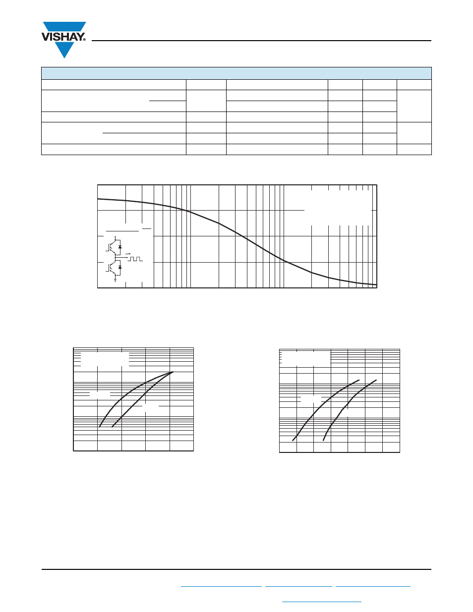
Fig. 1 - Typical Load Current vs. Frequency
(Load Current = I
RMS
of Fundamental)
Fig. 2 - Typical Output Characteristics
Fig. 3 - Typical Transfer Characteristics
THERMAL AND MECHANICAL SPECIFICATIONS
PARAMETER
SYMBOL
TEST CONDITIONS
TYP.
MAX. UNITS
Thermal resistance, junction to case
IGBT
R
thJC
-
0.24
°C/W
Diode
-
0.35
Thermal resistance, case to sink per module
R
thCS
0.1
-
Mounting torque
case to heatsink
-
4.0
Nm
case to terminal 1, 2 and 3
For screws M5 x 0.8
-
3.0
Weight of module
200
-
g
0.1
1
10
100
0
25
50
75
100
f - Frequency (kHz)
Load Current (A)
Duty cycle: 50 %
T
J
= 125 °C
T
sink
= 90 °C
Gate drive as specified
Power dissipation = 170 W
Ideal diodes
60 % of rated
voltage
Square wave:
-
0.5
1.0
1.5
2.0
2.5
3.0
1
10
100
1000
V
GE
= 15 V
500 µs pulse width
25 °C
125 °C
V
CE
- Collector to Emitter Voltage (V)
I
C
- Collector Current (A)
4.0
4.5
5.0
5.5
6.0
6.5
7.0
7.5
1
10
100
1000
V
GE
- Gate to Emitter Voltage (V)
I
C
- Collector to Emitter Current (A)
V
GE
= 20 V
500 µs pulse width
125 °C
25 °C