Vishay semiconductors, Electrical specifications (t, Switching characteristics (t – C&H Technology VS-GA250SA60S User Manual
Page 3: 25 °c unless otherwise specified)
VS-GA250SA60S
www.vishay.com
Vishay Semiconductors
Revision: 20-Jul-12
2
Document Number: 94704
For technical questions within your region:
,
,
THIS DOCUMENT IS SUBJECT TO CHANGE WITHOUT NOTICE. THE PRODUCTS DESCRIBED HEREIN AND THIS DOCUMENT
ARE SUBJECT TO SPECIFIC DISCLAIMERS, SET FORTH AT
www.vishay.com/doc?91000
Notes
(1)
Pulse width
80 μs; duty factor 0.1 %
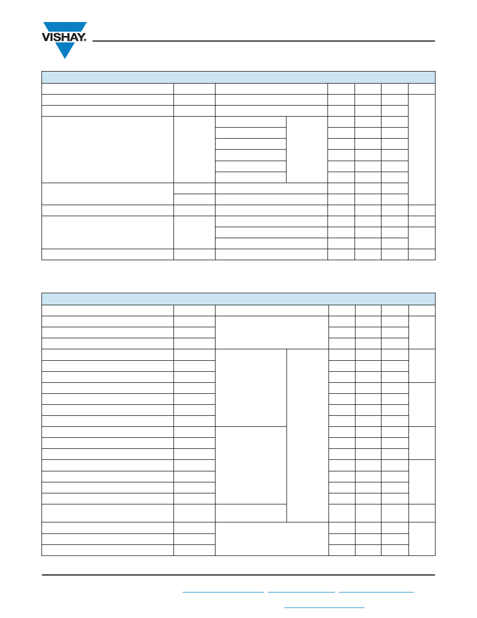
ELECTRICAL SPECIFICATIONS (T
J
= 25 °C unless otherwise noted)
PARAMETER SYMBOL
TEST
CONDITIONS
MIN.
TYP.
MAX.
UNITS
Collector to emitter breakdown voltage
V
(BR)CES
V
GE
= 0 V, I
C
= 1 mA
600
-
-
V
Emitter to collector breakdown voltage
V
(BR)ECS
(1)
V
GE
= 0 V, I
C
= 1.0 A
18
-
-
Collector to emitter voltage
V
CE(on)
I
C
= 100 A
V
GE
= 15 V
-
1.10
1.3
I
C
= 200 A
-
1.33
1.66
I
C
= 100 A, T
J
= 125 °C
-
1.02
-
I
C
= 200 A, T
J
= 125 °C
-
1.32
-
I
C
= 100 A, T
J
= 150 °C
-
1.02
-
I
C
= 200 A, T
J
= 150 °C
-
1.33
-
Gate threshold voltage
V
GE(th)
V
CE
= V
GE
, I
C
= 250 μA
3.0
4.5
6.0
V
CE
= V
GE
, I
C
= 250 μA, T
J
= 125 °C
-
3.1
-
Temperature coefficient of threshold voltage
V
GE(th)
/
T
J
V
CE
= V
GE
, I
C
= 1 mA, 25 °C to 125 °C
-
- 12
-
mV/°C
Collector to emitter leakage current
I
CES
V
GE
= 0 V, V
CE
= 600 V
-
20
1000
μA
V
GE
= 0 V, V
CE
= 600 V, T
J
= 125 °C
-
0.2
-
mA
V
GE
= 0 V, V
CE
= 600 V, T
J
= 150 °C
-
0.6
10
Gate to emitter leakage current
I
GES
V
GE
= ± 20 V
-
-
± 250
nA
SWITCHING CHARACTERISTICS (T
J
= 25 °C unless otherwise specified)
PARAMETER SYMBOL
TEST
CONDITIONS MIN.
TYP.
MAX.
UNITS
Total gate charge (turn-on)
Q
g
I
C
= 100 A, V
CC
= 600 V, V
GE
= 15 V
-
770
1200
nC
Gate-to-emitter charge (turn-on)
Q
ge
-
100
150
Gate-to-collector charge (turn-on)
Q
gc
-
260
380
Turn-on switching loss
E
on
T
J
= 25 °C
I
C
= 100 A
V
CC
= 480 V
V
GE
= 15 V
R
g
= 5.0
L = 500 μH
Energy
losses
include tail
and diode
recovery.
Diode used
60APH06
-
0.55
-
mJ
Turn-off switching loss
E
off
-
25
-
Total switching loss
E
tot
-
25.5
-
Turn-on delay time
t
d(on)
-
267
-
ns
Rise time
t
r
-
42
-
Turn-off delay time
t
d(off)
-
310
-
Fall time
t
f
-
450
-
Turn-on switching loss
E
on
T
J
= 125 °C
I
C
= 100 A
V
CC
= 480 V
V
GE
= 15 V
R
g
= 5.0
L = 500 μH
-
0.67
-
mJ
Turn-off switching loss
E
off
-
43.0
-
Total switching loss
E
tot
-
43.7
-
Turn-on delay time
t
d(on)
-
275
-
ns
Rise time
t
r
-
50
-
Turn-off delay time
t
d(off)
-
350
-
Fall time
t
f
-
700
-
Internal emitter inductance
L
E
Between lead and
center of die contact
-
5.0
-
nH
Input capacitance
C
ies
V
GE
= 0 V , V
CC
= 30 V, f = 1.0 MHz
-
16 250
-
pF
Output capacitance
C
oes
-
1040
-
Reverse transfer capacitance
C
res
-
190
-