Vishay high power products – C&H Technology GA75TS12UPbF User Manual
Page 5
www.vishay.com
For technical questions, contact: [email protected]
Document Number: 94427
4
Revision: 18-Jan-08
GA75TS120UPbF
Vishay High Power Products
"Half-Bridge" IGBT INT-A-PAK
(Ultrafast Speed IGBT), 75 A
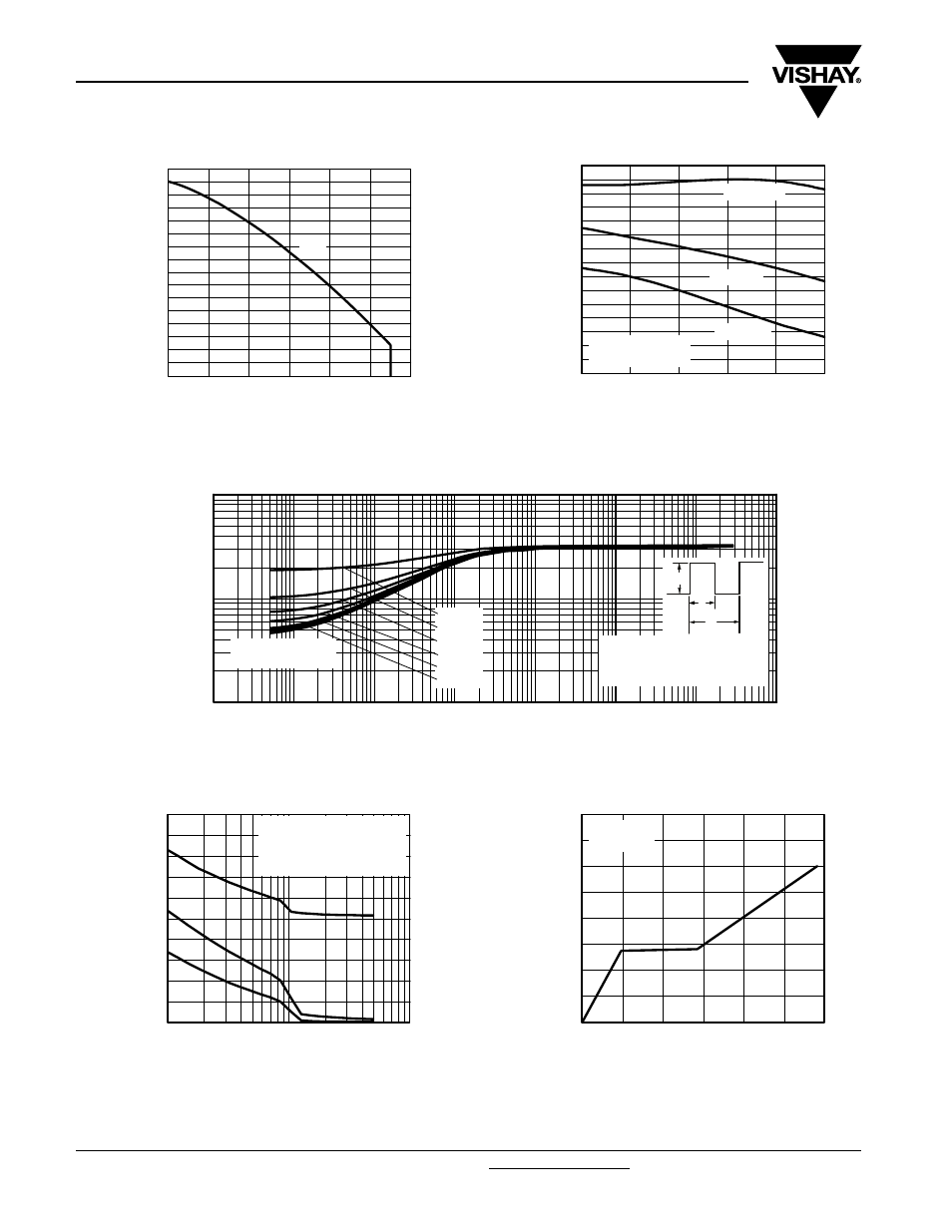
Fig. 4 - Case Temperature vs.
Maximum Collector Current
Fig. 5 - Typical Collector to Emitter Voltage vs.
Junction Temperature
Fig. 6 - Maximum Effective Transient Thermal Impedance, Junction to Case
Fig. 7 - Typical Capacitance vs.
Collector to Emitter Voltage
Fig. 8 - Typical Gate Charge vs. Gate to Emitter Voltage
0
20
40
80
100
120
0
20
40
60
80
100
120
140
160
T
C
- Case Temperature (°C)
Maximum DC Collector Current (A)
DC
60
1.5
2.0
3.0
0
30
60
90
120
150
T
J
- Junction Temperature (°C)
V
CE
- Collector to Emitter Voltage (V)
2.5
I
C
= 150 A
I
C
= 37 A
I
C
= 75 A
V
GE
= 15 V
500 µs pulse width
0.01
0.1
1
0.0001
0.001
0.01
0.1
1
t
1
- Rectangular Pulse Duration (s)
Z
thJC -
Thermal Response
10
100
1000
P
DM
t
1
t
2
Notes:
1. Duty factor D = t
1
/t
2
2. Peak T
J
= P
DM
x Z
thJC
+ T
C
Single pulse
(thermal response)
D = 0.50
D = 0.20
D = 0.10
D = 0.05
D = 0.02
D = 0.01
1
10
100
0
V
CE
- Collector to Emitter Voltage (V)
C - Capacitance (pF)
5000
10 000
15 000
20 000
25 000
V
GE
= 0 V, f = 1 MHz
C
ies
= C
ge
+ C
gc
, C
ce
shorted
C
res
= C
gc
C
oes
= C
ce
+ C
gc
0
200
400
600
0
5
10
15
20
Q
G
- Total Gate Charge (nC)
V
GE
- Gate to Emitter Voltage (V)
V
CC
= 400 V
I
C
= 85 A