4 board layout, 1 layout, Equation 2 – Texas Instruments TPS65023B User Manual
Page 6

)
R
R
(
max)
,
VLDO
REF
_
V
(
))
R
R
(
REF
_
V
min
,
DCDC
_
Vout
3
1
2
2
1
1
2
´
-
+
+
´
=
)
R
R
(
min)
,
VLDO
REF
_
V
(
))
R
R
(
REF
_
V
max
,
DCDC
_
Vout
3
1
2
2
1
1
2
´
-
+
+
´
=
Board Layout
www.ti.com
(2)
(3)
The most straight forward way is to choose a value for R6 according to the recommendations in the
converter data sheet.
4
Board Layout
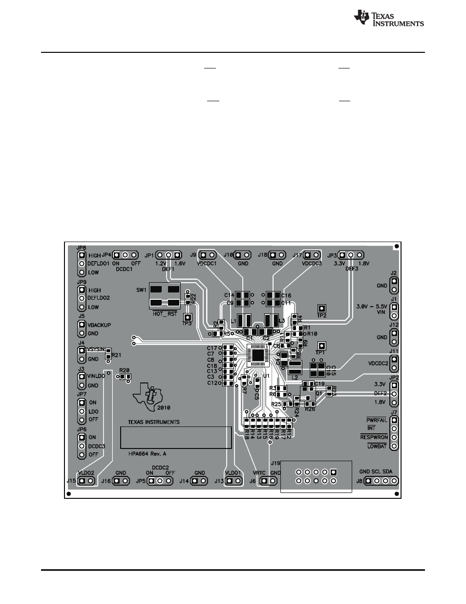
This section provides the TPS65023B/TPS650231EVM-664 board layout and illustrations.
4.1
Layout
Board layout is critical for all switch mode power supplies.
through
show the board
layout for the TPS65023B/TPS650231EVM-664 PCB. The nodes with high switching frequencies and
currents are short and are isolated from the noise-sensitive feedback circuitry. Careful attention has been
given to the routing of high-frequency current loops. See the data sheet for specific layout guidelines.
Figure 1. Assembly Layer
6
TPS65023B/TPS650231EVM
SLVU394 – October 2010
Copyright © 2010, Texas Instruments Incorporated
