3 ucc2891evm electrical performance specifications, 4 schematic – Texas Instruments UCC2891 User Manual
Page 5
www.ti.com
3
UCC2891EVM Electrical Performance Specifications
4
Schematic
UCC2891EVM Electrical Performance Specifications
The UCC2891EVM electrical performance specifications are listed in
.
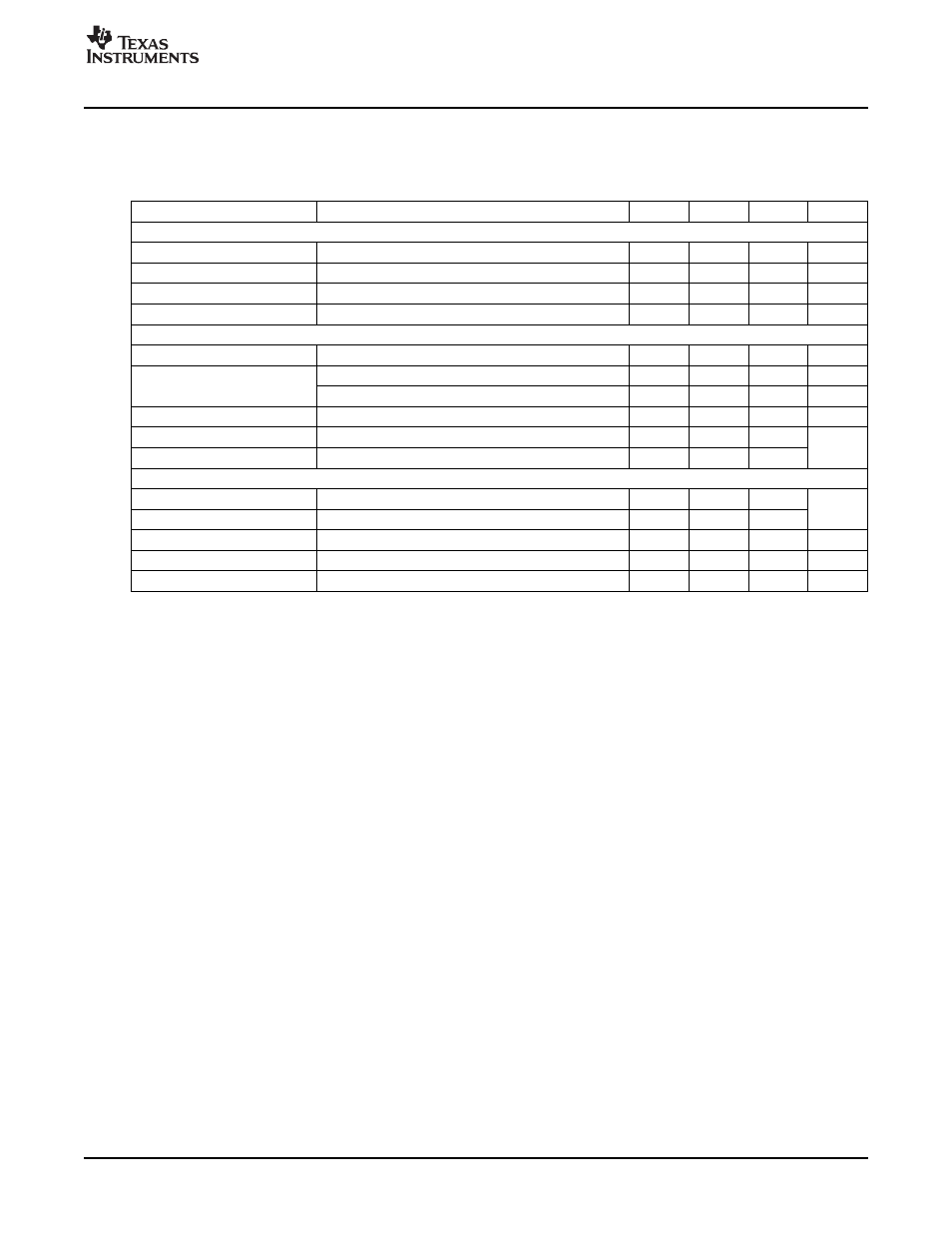
Table 1. UCC2891EVM Performance Summary
PARAMETER
TEST CONDITIONS
MIN
TYP
MAX
UNITS
Input Characteristics
Input voltage range
36
48
72
V
No load intput current
V
IN
= 36 V, I
OUT
= 0 A
75
100
mA
Maximum input current
V
IN
= 36 V, I
OUT
= 30 A
3.00
3.25
A
Input voltage ripple
V
IN
= 72 V, I
OUT
= 30 A
1.50
1.75
V
P-P
Input voltage ripple
Output voltage
36 V
≤
V
IN
≤
72 V, 0 A
≤
I
OUT
≤
30 A
3.25
3.30
3.35
V
Output voltage regulation
Line regulation (36 V
≤
V
IN
≤
72 V, I
OUT
= 0 A)
0.003%
Load regulation (0 A
≤
I
OUT
≤
30 A, V
IN
= 48 V)
0.060%
Output voltage ripple
V
IN
= 48 V, I
OUT
= 30 A
30
35
mV
P-P
Output load current
V
IN
= 48 V, I
OUT
= 30 A
0
30
A
Output current limit
36 V
≤
V
IN
≤
72 V
32
Output current limit
Switching frequency
275
325
kHz
Control loop bandwidth
36 V
≤
V
IN
≤
72 V, I
OUT
= 10 A
5
8
Control loop bandwidth
36 V
≤
V
IN
≤
72 V, 2 A
≤
I
OUT
≤
30 A
30
50
°
C
Peak efficiency
92%
Full load efficiency
V
IN
= 48 V, I
OUT
= 30 A
89%
A schematic of the UCC2891EVM is shown in
. Terminal block J1 is the 48-V input voltage source
connector and J8 is the output and return for the 3.3-V output voltage.
On the primary side, U1 is the UCC2891 shown with the necessary discrete circuitry for configuring the
controller to operate at 300 kHz with the maximum duty clamp set for 0.65. The EVM is programmed to
start at VIN=36 V, as determined by R11 and R12. To minimize power dissipation in the current sense, a
current sense transformer, T1 is used, as opposed to simply using a sense resistor between the source of
Q2 and power ground. Q2 is the primary switching MOSFET and is selected based upon VDS and low
RDS(on). Q1 is the AUX (active reset) MOSFET and is selected based upon preferred package only, with
only minor consideration given for R
DS(on)
and Qg. Since the active clamp used in this design is low-side
referenced, Q1 must be a P-channel type MOSFET. The reason for this is further explained in application
note SLUA299[2]. C9 is the clamp capacitor used to maintain a constant dc voltage. The input voltage is
subtracted from the clamp voltage to allow transformer reset during the active clamp period.
SLUU178A – November 2003 – Revised December 2006
Using the UCC2891 Active Clamp Current Mode PWM Controller
5