Texas Instruments PGA309EVM-USB User Manual
Page 9

www.ti.com
System Setup
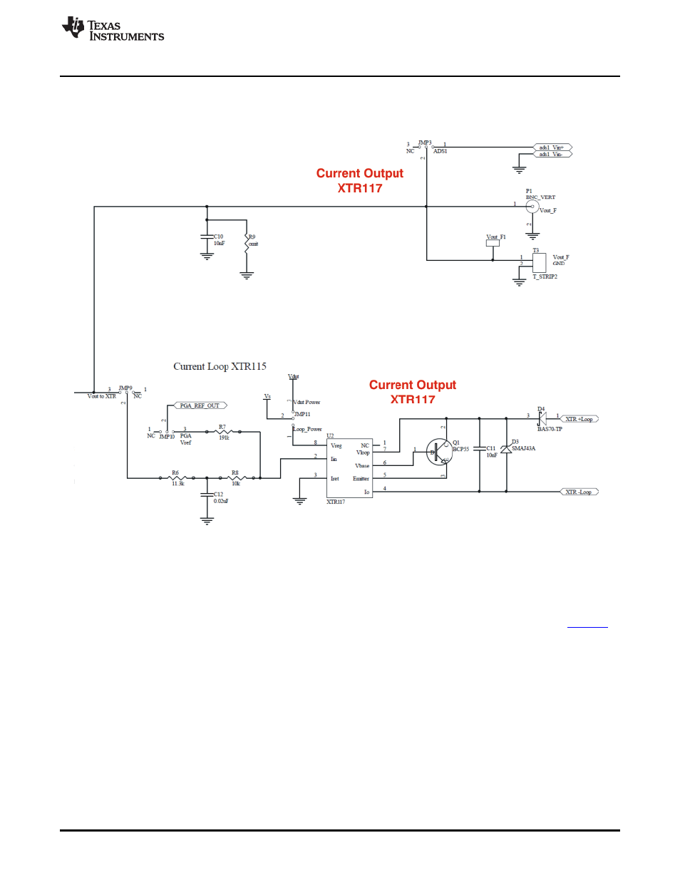
shows the output section of the PGA309EVM_Test_Board. There are two output options: voltage
output and current output. The voltage output option is selected by placing JMP9 in the NC position. The
current output option is selected by moving JMP9 to the V
OUT
to XTR position.
Figure 6. PGA309_Test_Board Schematic: Output Circuitry
In voltage output mode, C10 = 10nF is connected to the PGA309 output. This capacitor is used for radio
frequency interference (RFI) and electromagnetic interference (EMI) immunity. This component should be
included in your design, if possible.
In current output mode, the PGA309 output is connected to a voltage-to-current (V-I) converter (
The sum of R6 and R8 convert the output voltage from the PGA309 to an input current for the XTR117.
R7 can be used to create an input offset current using the reference. The total input current is I
IN
= V
OUT
/
(R6 + R8) + V
REF
/R7. The output current is equal to the input current times the current gain (x 100).
D4 is used for reverse polarity protection. D3 is used for over-voltage transient protection. D3 was
selected for low leakage. Leakage on D3 directly contributes to error. C11 is a decoupling capacitor and is
required for proper operation. The external transistor, Q1, conducts the majority of the full-scale output
current. Power dissipation in this transistor can approach 0.8W with high loop voltage (40V) and 20mA
output current.
9
SBOU084 – February 2010
PGA309EVM-USB
Copyright © 2010, Texas Instruments Incorporated
