Figure 2–6. output ripple voltage detail – Texas Instruments SLVU013 User Manual
Page 38
External Component Selection
2-18
Figure 2–6. Output Ripple Voltage Detail
(a)
Current waveform through output capacitor
(b)
Voltage waveform across ideal capacitor with initial value at
beginning of high-side MOSFET on-time
V
C
+
D
I
t2
2
Co
D
Ts
–
D
I
t
2
Co
High-side MOSFET ON
High-side MOSFET OFF
V
C
+ D
I
t
2
Co
–
D
I
t2
2
Co
(1–D)
Ts
(c)
Voltage waveform across ESR
V
ESR
+
ESR
D
I
t
D
Ts
–
D
I
2
High-side MOSFET ON
High-side MOSFET OFF
V
ESR
+
ESR
D
I
2
–
D
I
t
(1
–D)
Ts
(d)
Voltage waveform across ESL
V
ESL
+
ESL
D
I
D
Ts
High-side MOSFET ON
High-side MOSFET OFF
V
ESL
+
–
ESL
D
I
(1
–D)
Ts
Hyst
(a)
(b)
(c)
(d)
(e)
IAC
∆Ι
VC
VESR
VESL
Vripple
tdel
t
t
t
t
tdel t
Vp–p
ton
toff
Ts
(e)
Composite output voltage ripple waveform
V
ripple
+
V
C
)
V
ESR
)
V
ESL
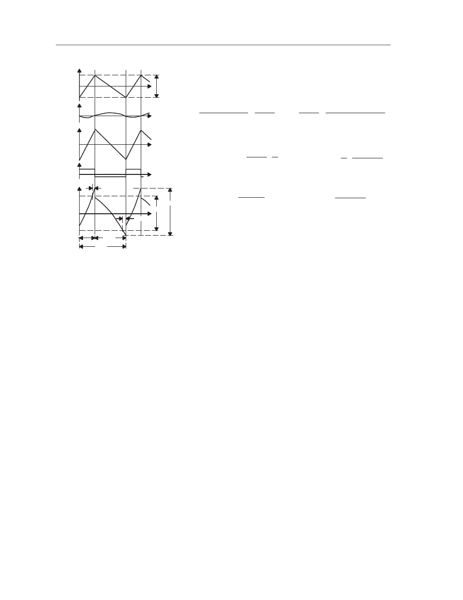
Figures 3–6, 3–15, 3–24, and 3–33 show the phase voltage (voltage at
junction of high-side MOSFET with low-side MOSFET), and output voltage
ripple waveforms for the example circuit of Figure 1–3. The output voltage
waveform is slightly different from the theoretical waveform of Figure 2–6(e)
due to the smoothing effect of the 10-
µ
F ceramic capacitor in parallel with the
electrolytic capacitors.
2.2.4.2
Switching Frequency Equation
Assume that the input and output voltage ripple magnitudes are relatively
negligible compared to the dc component. Also assume that the time constant
L/(R
DS(on)
+ R
L
), where L is the output inductance, R
L
is the inductor resistance
and R
DS(on)
is the on-state resistance of the high-side MOSFET(s), is high in
comparison with the switching period. Assume the body diode conduction time
and switching transition time are much smaller than the switching period.
These assumptions are reasonable for low voltage ripple and high efficiency
regulators. In such a case the output inductor current can be modeled as
the sum of the dc component, which is equal to the output current
Io, and
the ac linear ramp component, which flows through the output capacitor
[Figure 2–6(a)].
The numbered equations in this section are used to derive the switching
frequency equation.