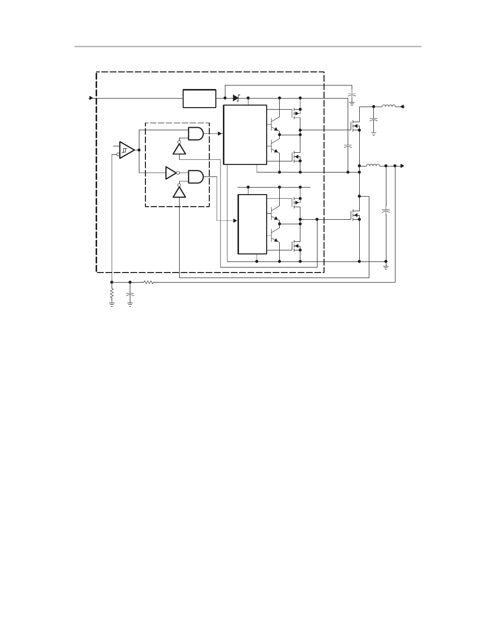
Figure 2–4. gate driver block diagram – Texas Instruments SLVU013 User Manual
Page 31

TPS56xx Functions
2-11
Design Procedure
Figure 2–4. Gate Driver Block Diagram
Level
Shifter/
Predriver
M1
45
Ω
M2
5
Ω
BOOT
HIGHDR
C4
BOOTLO
Highside Driver
Predriver
M3
45
Ω
M4
5
Ω
LOWDR
DRVGND
Lowside Driver
L2
Vphase
C2
VO
Vin
C1
L1
C3
DRV
8 V Drive
Regulator
Adaptive
Deadtime
Control
LOWDR
VREF
VCC
12 V
R2
R1
C5
TPS56xx Synchronous-Buck Controller
Figure 2–5 gives an I–V sweep of the low-side driver during sinking. The
Rds(on) of the MOS transistors for the sink stage is 5
Ω
at T
J
= 125
°
C and is
45
Ω
for the source stage. The Rds(on) is lower for the sink stage to provide
a low impedance path for the displacement current that flows through the Miller
capacitance of the power MOSFET when the drain switches. This is especially
important for the low-side driver to keep the low-side MOSFET off when the
high-side MOSFET is turned on.
