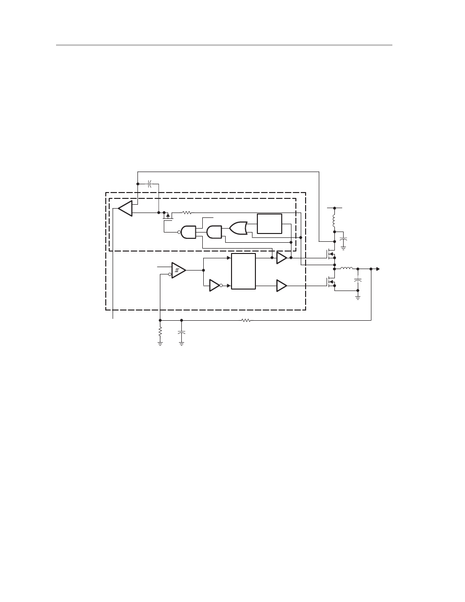
Figure 2–3. v, Sensing circuit, Tps56xx functions 2-8 – Texas Instruments SLVU013 User Manual
Page 28

TPS56xx Functions
2-8
Figure 1–3). This arrangement improves efficiency over solutions having a
separate current sensing resistor. The drain of the high-side MOSFET is
connected to HISENSE (pin 19). The source of the high-side MOSFET is
connected to LOSENSE (pin 20). When the high-side MOSFET is on, a
TPS56xx internal switch is also on and samples the source voltage of the
high-side MOSFET. This sampled voltage is applied to IOUTLO (pin 21) and
is held by the external 0.1-
µ
F capacitor, C6, which is connected from IOUTLO
(pin 21) to HISENSE (pin 19). The TPS56xx amplifies (gain=2) the
sampled-and-held voltage on C6 and sends the output voltage to IOUT (pin
1).
Figure 2–3. V
DS
Sensing Circuit
Adaptive
Deadtime
Control
HIGHDR
C1
L1
Vin
L2
C2
LOSENSE
LOWIN
Vphase
VO
TPS56xx Synchronous-Buck Controller
C3
R2
VSENSE
R1
+
–
IOUT
Rising
Edge
Delay
Vref
LOWDR
HIGHIN
Shutdown
IOUTLO
HISENSE
Cs/h
Gain of 2
Vds Sensing Circuit
Figure 2–3 gives a simple block diagram of the Vds sensing circuit. The Vds
sensing circuit measures the average voltage across the high-side MOSFET
when the high-side MOSFET is on, and holds that value on a sample/hold
capacitor when the high-side MOSFET is off. The voltage on the sample/hold
capacitor is directly proportional to the load current. Sensing across the
high-side MOSFET rather than the low-side MOSFET ensures that shorted
loads can be detected. The RC time constant of the sample/hold network must
be greater than the conduction-time of the high-side MOSFET, otherwise the
sample/hold circuit will function as a peak detector circuit and will not hold the
average Vds voltage. The differential voltage across the sample/hold
capacitor is amplified by 2 and converted to a single-ended signal on the IOUT
pin. The DC CMRR of the Vds sensing amplifier is 69 dB minimum. Added logic
ensures that sampling begins and ends while the high-side MOSFET is
conducting. The turn-on and turn-off delays of the sample/hold switch are less
than 100 ns. Additional logic and a rising edge delay circuit are included to
guarantee sampling during a short-to-ground fault across the low-side
MOSFET; the rising edge delay time is 500 ns.
Resistors R7 and R13 in Figure 1–3 set the current limit setpoint. This
resistor-divider network applies the IOUT output voltage to OCP (pin 3). The
