Quatech MPAP-100 User Manual
Page 55
N/C
N/C
RxCLK (DTE)
SYNCA
N/C
CD
DGND
DSR
CTS
RTS
RxD
TxD
CGND
13
12
11
10
9
8
7
6
5
4
3
2
1
25
24
23
22
21
20
19
18
17
16
15
14
TM (OUTPUT)
TxCLK (DTE)
N/C
N/C
RLBK (OUTPUT)
DTR
N/C
LLBK (OUTPUT)
RxCLK (DCE)
N/C
TxCLK (DCE)
RING
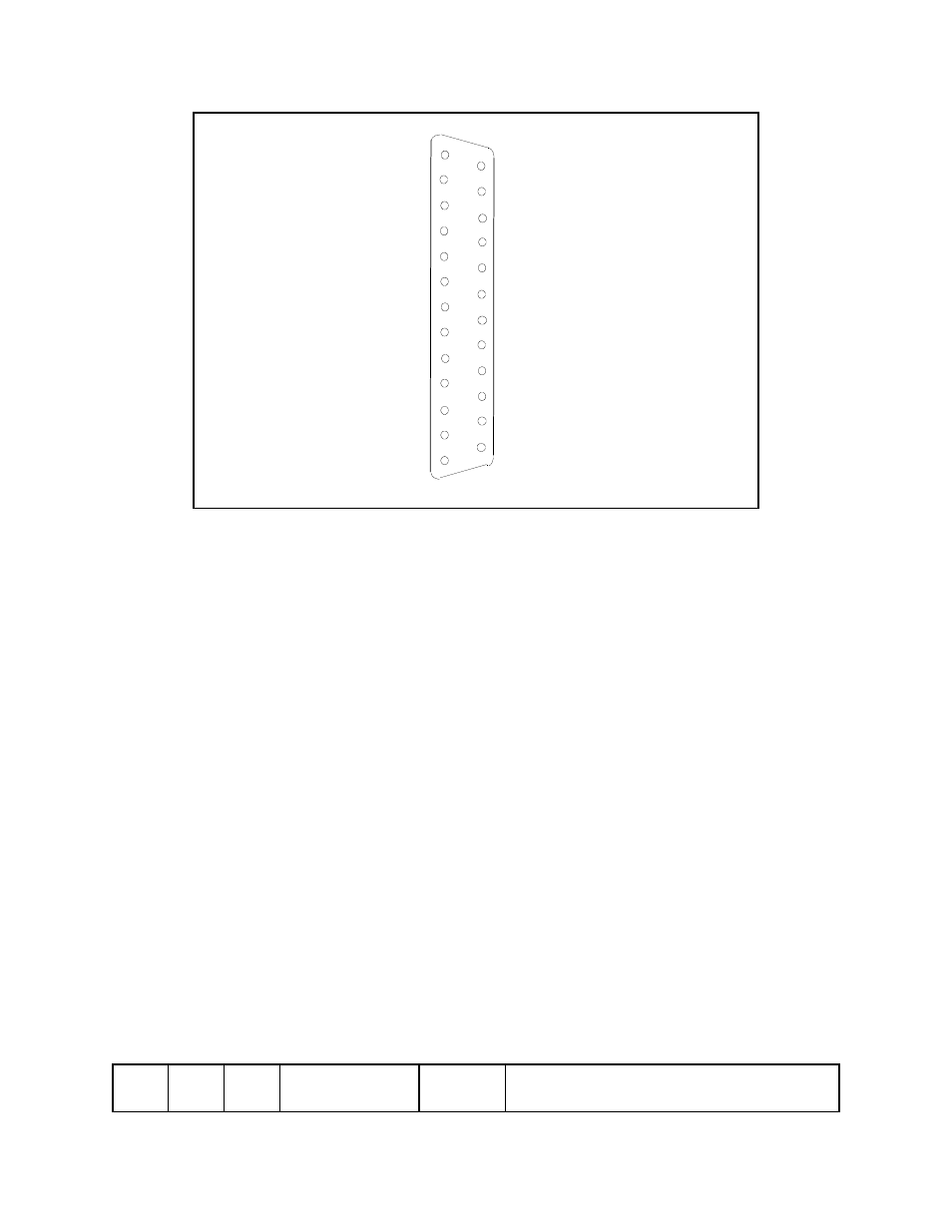
Figure 2 --- MPAP-100 Output Connector
The testing signals the DTE can generate are Local Loopback (LL) and Remote Loopback
(RL). These signals are asserted with certain bits in the Communications Register. When a Test
Mode (TM) condition is received from the DCE, an interrupt can optionally be generated.
19.1 SYNCA (pin 10)
If EXTSYNC (bit 6) in the Communications Register is set to a logic 1, the SYNCA
signal from the connector is used to drive the active-low SYNC input of SCC channel A. The
signal is inverted by the RS-232 receiver, so a positive voltage on pin 10 will assert SYNCA.
The SCC must be specifically programmed to recognize external synchronization.
19.2 RING (pin 22)
If Card and Socket Services has set the SIGCHG bit in the PCMCIA Configuration Status
Register to a logic 1, the RING signal is routed to the STSCHG line on the PCMCIA bus. The
signal is inverted by the RS-232 receiver, so a positive voltage on pin 22 will assert STSCHG.
Table 17 shows the pin configuration of the MPAP-100 DTE connector. The definitions
of the interchange circuits according to the RS-232-D standard can be found starting on page 52.
SCC Pin or Register Bit
RS-232-D
Circuit
Signal
From
DTE
To
DTE
Pin