13 appendix d – legacy pcb (rev 1.1) details, 1 i/o connector, 2 debounce links – Optiquest iRIS 320 User Manual
Page 69
67
-
iRIS 220 / iRIS 320, V1.19 User Guide
13 Appendix D – Legacy PCB (Rev 1.1) Details
13.1 I/O Connector
All I/O and power supply terminations on the V1.1 PCB are via 2.5mm (0.1”) screw terminals provided on a
12-way pluggable connector. This connector is positioned on the right hand side of the iRIS 320 circuit
board, directly above the white battery connector. On the iRIS 220, the connector protrudes through the top
of the case.
The function of each I/O termination is shown in the diagram below.
TOP
AI2
Analog Input #2
AI1
Analog Input #1
AGND Analog Common Ground
DI2
Digital Input #2
DI1
Digital Input #1
DO2
Digital Output #2
DO1
Digital Output #1
DGND Digital Common Ground
12V+
12Vdc Internal/External Battery Supply +
12V - 12Vdc Internal/External Battery Supply – (GND)
VIN+
15-30Vdc External Power Supply (Charger Input) +
GND (-) 0Vdc External Power Supply (Charger Input) -
BOTTOM
NOTE: The terminal marked 12V- is bonded to the other GND terminals and on the Revision 1.2 PCB is
marked as such.
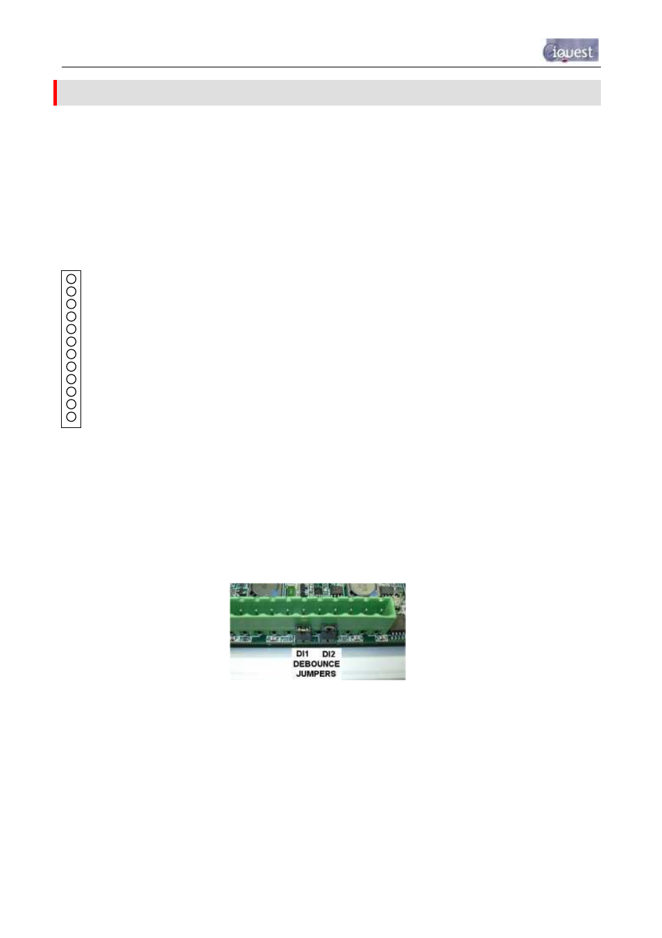
13.2 Debounce Links
The picture below shows the position of the debounce links on the Revision 1.1 PCB.
Figure 15 – V1.1 PCB Debounce Links