3 setting the switches – Renesas Temporary Target Board M38517T-ADS User Manual
Page 9
( 7 / 12 )
No.
SW1
SW2
SW3
Name
PORT/XCIN
VREF
CNVss
Function
Allows you to choose whether to supply the sub-clock
signals (32.768 kHz) to the MCU's XCIN pin (pin 16).
To use pin P21/XCIN as an I/O port, choose the PORT
side.
To use the sub-clock signals, choose the XCIN side.
Allows you to choose whether to apply Vcc or some
other source to the MCU's VREF pin (pin 2). In the
case of the latter, choose the J1-2 side, and apply a
voltage within a prescribed range to the J1-2.
Allows you to choose which to connect, Vcc or Vss, to
the MCU's CNVss (pin 15).
Factory-setting
PORT
Vcc
Vss
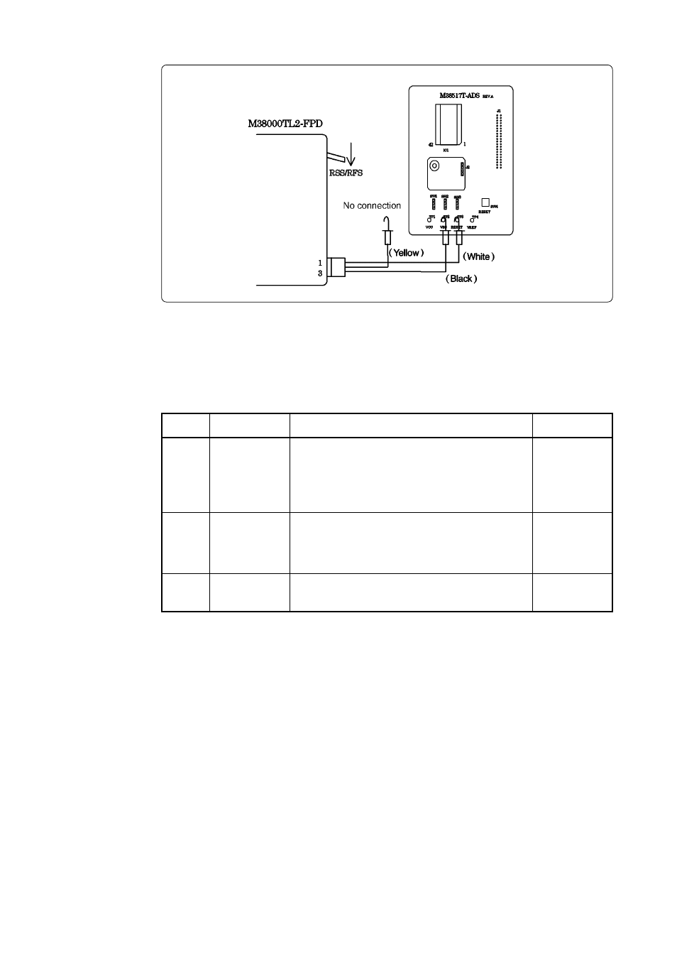
Figure 4.3 Connecting the M38517RSS
4.3 Setting the Switches
Set the switches SW1 to SW3 according to your applications. Table 4.3 describes the functions of
the switches SW1 to SW3.
Table 4.3 Functions of the switches SW1, SW2 and SW3
- Single-Chip Microcomputer M34551T2-MCU (42 pages)
- M3T-FLX-80NRA (6 pages)
- 70 (162 pages)
- M16C/30P (102 pages)
- PROM Programming Adapter PCA7427G02 (20 pages)
- R0E572110CFK00 (40 pages)
- H8/325 Series (20 pages)
- Single-Chip Microcomputer H8/36079 (27 pages)
- Direct Dummy IC M3T-DIRECT100S (4 pages)
- M3A-2152 (95 pages)
- PCA7755D (6 pages)
- M16C/6N5 (106 pages)
- SH7085 (50 pages)
- QFP-144 (23 pages)
- H8/3834 Series (22 pages)
- RSKM16C62P (3 pages)
- H8/33937 (22 pages)
- Single-Chip Microcomputer H8SX/1622 (5 pages)
- E6000 (29 pages)
- PCA7400 (18 pages)
- PCA4738FF-64 (20 pages)
- SuperH HS7339KCU01HE (43 pages)
- M16C FAMILY (103 pages)
- PCA7412F-100 (20 pages)
- 4513 (210 pages)
- M34551E8FP (16 pages)
- Dummy IC M3T-SSOP36B-450 (4 pages)
- Emulation Pod M30100T3-RPD-E (52 pages)
- Converter Board for M30102 M30102T-PTC (4 pages)
- SH7145 (31 pages)
- HS1653ECN61H (36 pages)
- Converter Board R0E521276CFG00 (4 pages)
- PCA7302E1F-80 (18 pages)
- H8/3814 Series (21 pages)
- H8S/2646 Series (20 pages)
- SuperHTM Family SH7125 Series (40 pages)
- M30262T-PTC (4 pages)
- SH7670 (82 pages)
- H8/3864 Series (20 pages)
- Emulator System M3T-MR100 (306 pages)
- 38K0 (6 pages)
- PLQP0176KB-A (40 pages)
- Direct Dummy IC M3T-DIRECT80S (6 pages)
- PCA4738L-80A (26 pages)
- Converter Board R0E5212BACFG00 (6 pages)