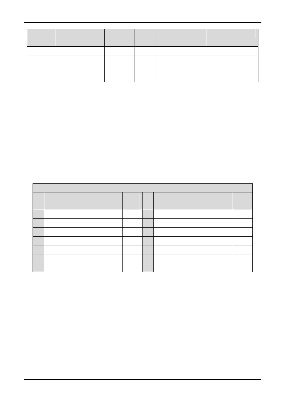
Debug lcd module, Table 6-3 – Renesas H8SX/1648 User Manual
Page 12
Description
Function
Circuit Net
Name
Device
Pin
Fit for RS232
Remove for RS232
SCI1
Programming serial port
TXD1
59
R31
R37, R32
SCI1
Programming serial port
RXD1
55
R30
R36, R33
SCI4
Spare Serial Port
TXD4
107
R37
R31, R32
SCI4
Spare Serial Port
RXD4
108
R36
R30, R33
Table 6-3: Serial Port settings
The SCI1 port is also available on J2 and JA2. The SCI4 port is available on J3.
6.5. Debug LCD Module
A debug LCD module is supplied to be connected to the connector LCD. This should be fitted so that the debug LCD module lies over J3.
Care should be taken to ensure the pins are inserted correctly into LCD. The debug LCD module uses a 4 bit interface to reduce the pin
allocation. No contrast control is provided; this is set by a resistor on the supplied display module. The module supplied with the RSK only
supports 5V operation.
Table 6-4 shows the pin allocation and signal names used on this connector.
LCD
Pin
Circuit Net Name
Device
Pin
Pin
Circuit Net Name
Device
Pin
1 Ground
-
2 5V
Only
-
3 No
Connection
-
4
DLCDRS (P33)
62
5
R/W (Wired to Write only)
-
6
DLCDE + 100k pull down to ground (PC4)
47
7 No
Connection
-
8 No
connection
-
9 No
Connection
-
10 No
connection
-
11
DLCDD4 (PC0)
45
12
DLCDD5 (PC1)
46
13
DLCDD6 (PC2)
116
14
DLCDD7 (PC3)
117
Table 6-4 Debug LCD Module Connections
10