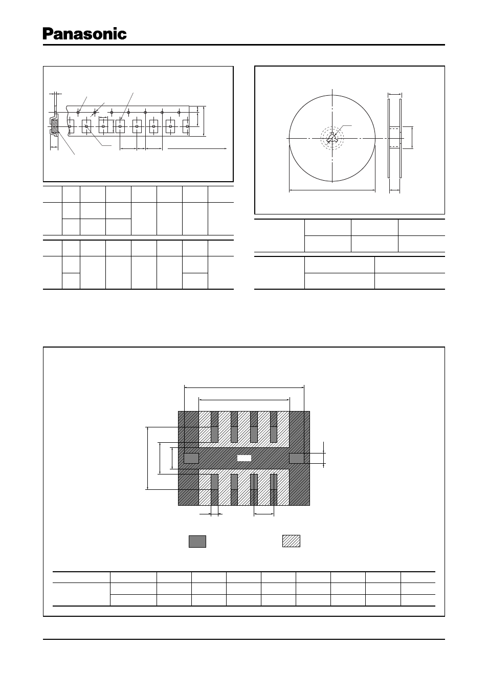
Chip 3-terminal capacitor array, Recommended land pattern design – Panasonic EZASC User Manual
Page 4

Chip 3-Terminal Capacitor Array
Design and specifi cations are each subject to change without notice. Ask factory for the current technical specifi cations before purchase and/or use.
Should a safety concern arise regarding this product, please be sure to contact us immediately.
t
1
t
2
Chip component
P
1
P
2
P
0
Compartment
Sprocket hole
fD
0
Tape running direction
E
F
W
A
B
fD
1
f
B
W
T
fA
fC
GND
c
f2
f1
a
e
d
b
P
Land pattern
Solder resistant
● Embossed Carrier Taping
● Taping Reel
■
Recommended Land Pattern Design
Chip 3-Terminal Capacitor Array
(EZANC/EZASC)
Type
A
B
W
F
E
P
0
Dimensions
(mm)
EZASC 2.50
±0.20
4.40
±0.20
12.00
±0.30
5.50
±0.20
1.75
±0.20
4.00
±0.10
EZANC 3.50
±0.20
6.80
±0.20
Type
P
1
P
2
fD
0
t
1
t
2
fD
1
Dimensions
(mm)
EZASC
4.00
±0.10
2.00
±0.05
1.50
+0.10
0.25
±0.05
1.15
±0.20
1.50
+0.10
EZANC
1.30
±0.20
−0
−0
Dimensions
(mm)
fA
fB
fC
180
+0
60 min.
13.0
±1.0
Dimensions
(mm)
W
T
13.0
±1.0
15.4
±2.0
−3.0
Type
a
b
c
d
e
f1
f2
P
Dimensions
(mm)
EZASC
1.2 to 1.4
0.4
3.1 to 3.3 0.4 to 0.5
0.8
2.9 to 3.3 4.8 to 5.2
0.8
EZANC
2.2 to 2.4 0.4 to 0.6 5.7 to 5.9 0.4 to 0.8
1.8
4.2 to 4.6 7.5 to 7.9
1.27
Feb. 2006
