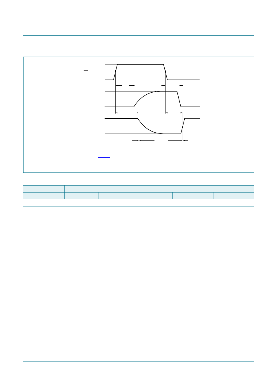
Figure 12, Table 9, Cbtd3306 – Philips CBTD3306 User Manual
Page 8: Nxp semiconductors, Dual bus switch with level shifting

CBTD3306
All information provided in this document is subject to legal disclaimers.
© NXP B.V. 2012. All rights reserved.
Product data sheet
Rev. 8 — 1 May 2012
8 of 17
NXP Semiconductors
CBTD3306
Dual bus switch with level shifting
Measurement points are given in
.
Logic levels: V
OL
and V
OH
are typical output voltage levels that occur with the output load.
Fig 12. Enable and disable times
001aak298
t
PLZ
t
PHZ
outputs
disabled
outputs
enabled
V
Y
V
X
outputs
enabled
output
LOW to OFF
OFF to LOW
output
HIGH to OFF
OFF to HIGH
nOE input
V
I
3.5 V
V
M
V
M
V
OL
V
OH
GND
GND
t
PZL
t
PZH
V
M
V
M
Table 9.
Measurement points
Supply voltage
Input
Output
V
CC
V
I
V
M
V
M
V
X
V
Y
V
CC
= 5.0 V
± 0.5 V GND to 3.0 V
1.5 V
1.5 V
V
OL
+ 0.3 V
V
OH
− 0.3 V
See also other documents in the category Philips Computer Accessories:
- WUB1110 (12 pages)
- WUB1110 (12 pages)
- PTA01 (2 pages)
- BUK205-50Y (13 pages)
- SPA5210 (7 pages)
- SDC5100/27 (7 pages)
- US2-PH1620 (2 pages)
- SPP3201WC (2 pages)
- FR-996 (33 pages)
- FR-994 (84 pages)
- SWV1010 (2 pages)
- SWV3053 (2 pages)
- SWS3412W/10 (2 pages)
- SPP1182WC (2 pages)
- SWS6813T (2 pages)
- SWV2030/97 (2 pages)
- SWS2822T/17 (2 pages)
- LEDINO 31602/**/16 (40 pages)
- SWV3573/10 (2 pages)
- SBC SP 370 (46 pages)
- Theatre Director SPP4220 (12 pages)
- SPP1187WC (2 pages)
- MBD127 (9 pages)
- SWV2052W (2 pages)
- SPP2304WC (2 pages)
- SPP1187WA (2 pages)
- MAGNAVOX 26MD357B/37 (2 pages)
- SPP3226WA (2 pages)
- FMXXFD20B (10 pages)
- Slimline SPP1180WA/37 (2 pages)
- BUK216-50YT (8 pages)
- Universal Serial Bus ISP1122 (48 pages)
- SPD2410BD (2 pages)
- SPP4410WA (2 pages)
- SPP7344WA (2 pages)
- SWS7683W/10 (2 pages)
- SWV2564 (2 pages)
- SPP2307WC (2 pages)
- SPP5126A/17 (8 pages)
- SWV2052 (2 pages)
- SPP4031A/17 (2 pages)
- SWS3435S/27 (12 pages)
- SWV3571/10 (2 pages)
- SWS3412/10 (2 pages)
- BUK209-50Y (8 pages)
