Static characteristics, Cbtd3306, Nxp semiconductors – Philips CBTD3306 User Manual
Page 4
CBTD3306
All information provided in this document is subject to legal disclaimers.
© NXP B.V. 2012. All rights reserved.
Product data sheet
Rev. 8 — 1 May 2012
4 of 17
NXP Semiconductors
CBTD3306
Dual bus switch with level shifting
10. Static characteristics
[1]
All typical values are at V
CC
= 5 V, T
amb
= 25
°C.
[2]
This is the increase in supply current for each input that is at the specified TTL voltage level rather than V
CC
or GND.
[3]
Measured by the voltage drop between the nA and the nB terminals at the indicated current through the switch. ON resistance is
determined by the lowest voltage of the two (nA or nB) terminals.
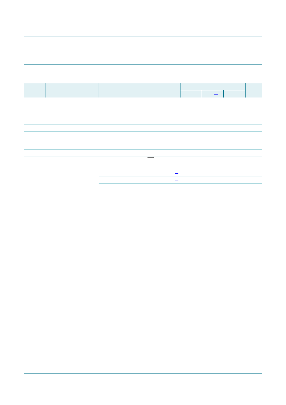
Table 7.
Static characteristics
Voltages are referenced to GND (ground = 0 V).
Symbol
Parameter
Conditions
T
amb
=
−40 °C to +85 °C
Unit
Min
Typ
Max
V
IK
input clamping voltage
V
CC
= 4.5 V; I
I
=
−18 mA
-
-
−1.2
V
I
I
input leakage current
V
CC
= 5.5 V; V
I
= GND or 5.5 V
-
-
±1
μA
I
CC
supply current
V
CC
= 5.5 V; I
SW
= 0 mA;
V
I
= V
CC
or GND
-
-
1.5
mA
V
pass
pass voltage
see
-
-
-
V
ΔI
CC
additional supply current
per input pin; V
CC
= 5.5 V;
one input at 3.4 V, other inputs at
V
CC
or GND
-
-
2.5
mA
C
I
input capacitance
control pin; V
I
= 3 V or 0 V
-
3.2
-
pF
C
io(off)
off-state input/output
capacitance
port off; V
I
= 3 V or 0 V; nOE = V
CC
-
6.5
-
pF
R
ON
ON resistance
V
CC
= 4.5 V; V
I
= 0 V; I
I
= 64 mA
-
3.6
5
Ω
V
CC
= 4.5 V; V
I
= 0 V; I
I
= 30 mA
-
3.6
5
Ω
V
CC
= 4.5 V; V
I
= 2.4 V; I
I
= 15 mA
-
17
35
Ω