Package outline, Cbtd3306, Nxp semiconductors – Philips CBTD3306 User Manual
Page 10: Dual bus switch with level shifting
CBTD3306
All information provided in this document is subject to legal disclaimers.
© NXP B.V. 2012. All rights reserved.
Product data sheet
Rev. 8 — 1 May 2012
10 of 17
NXP Semiconductors
CBTD3306
Dual bus switch with level shifting
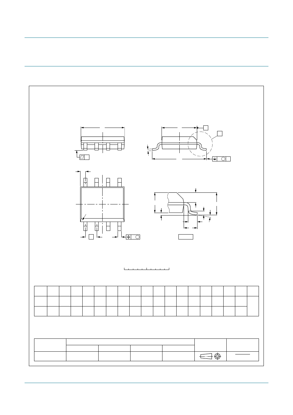
14. Package outline
Fig 14. Package outline SOT96-1 (SO8)
UNIT
A
max.
A
1
A
2
A
3
b
p
c
D
(1)
E
(2)
(1)
e
H
E
L
L
p
Q
Z
y
w
v
θ
REFERENCES
OUTLINE
VERSION
EUROPEAN
PROJECTION
ISSUE DATE
IEC
JEDEC
JEITA
mm
inches
1.75
0.25
0.10
1.45
1.25
0.25
0.49
0.36
0.25
0.19
5.0
4.8
4.0
3.8
1.27
6.2
5.8
1.05
0.7
0.6
0.7
0.3
8
0
o
o
0.25
0.1
0.25
DIMENSIONS (inch dimensions are derived from the original mm dimensions)
Notes
1. Plastic or metal protrusions of 0.15 mm (0.006 inch) maximum per side are not included.
2. Plastic or metal protrusions of 0.25 mm (0.01 inch) maximum per side are not included.
1.0
0.4
SOT96-1
X
w
M
θ
A
A
1
A
2
b
p
D
H
E
L
p
Q
detail X
E
Z
e
c
L
v
M
A
(A )
3
A
4
5
pin 1 index
1
8
y
076E03
MS-012
0.069
0.010
0.004
0.057
0.049
0.01
0.019
0.014
0.0100
0.0075
0.20
0.19
0.16
0.15
0.05
0.244
0.228
0.028
0.024
0.028
0.012
0.01
0.01
0.041
0.004
0.039
0.016
0
2.5
5 mm
scale
SO8: plastic small outline package; 8 leads; body width 3.9 mm
SOT96-1
99-12-27
03-02-18