Package outline – Philips BGD502 User Manual
Page 5
2001 Nov 15
5
NXP Semiconductors
Product specification
550 MHz, 18.5 dB gain power doubler
amplifier
BGD502
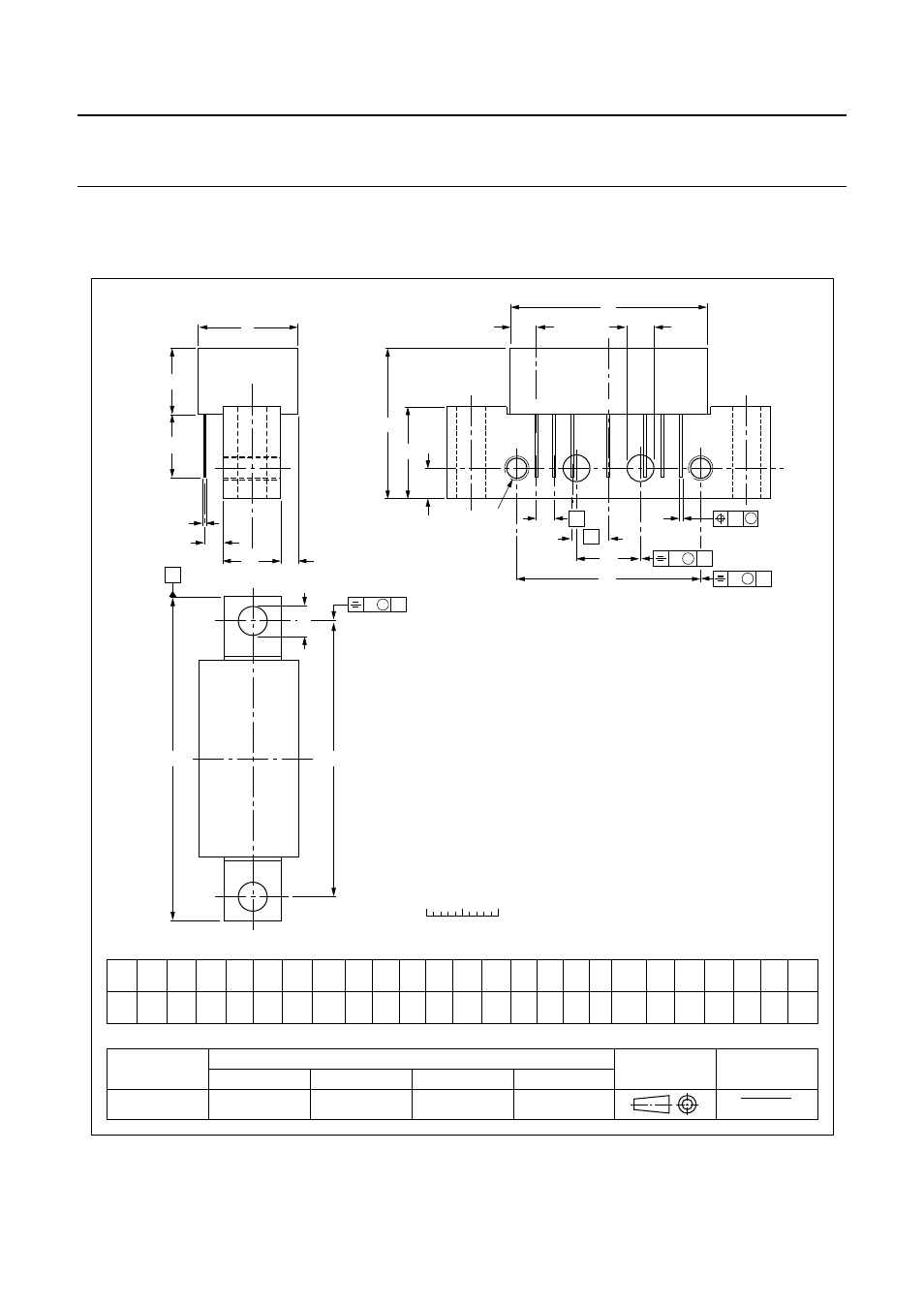
PACKAGE OUTLINE
UNIT
A2
max.
c
e
e1
q
Q
max.
q1
q2
U2
U1
W
REFERENCES
OUTLINE
VERSION
EUROPEAN
PROJECTION
ISSUE DATE
IEC
JEDEC
JEITA
mm
20.8
9.5
0.51
0.38
0.25 27.2
2.04
2.54
13.75 2.54 5.08 12.7 8.8
4.15
3.85
2.4
38.1 25.4 10.2 4.2
44.75
44.25
8.2
7.8
0.25
0.1
3.8
b
F
p
6-32
UNC
y
w
0.7
x
S
DIMENSIONS (mm are the original dimensions)
SOT115J
0
5
10 mm
scale
A
max.
D
max.
L
min.
E
max.
Z
max.
Rectangular single-ended package; aluminium flange; 2 vertical mounting holes;
2 x 6-32 UNC and 2 extra horizontal mounting holes; 7 gold-plated in-line leads
SOT115J
D
U1
q
q2
q1
b
F
S
A
Z
p
E
A2
L
c
d
Q
U2
M
w
7
8
9
2
3
W
e
e1
5
p
1
d
x
M
B
y
M
B
B
04-02-04
10-06-18
y
M
B
See also other documents in the category Philips Receivers and Amplifiers:
- SA58605 (9 pages)
- TDA1596T (22 pages)
- UA741C (7 pages)
- BGX885N (8 pages)
- TDA8946J (23 pages)
- BGY280 (11 pages)
- SWS2083W/17 (2 pages)
- MC1558 (6 pages)
- BGY148B (12 pages)
- HTR5205 (3 pages)
- TDA8559T (36 pages)
- TDA8542 (20 pages)
- TDA7056A (9 pages)
- TDA1552Q (10 pages)
- TDA7052A (12 pages)
- Audio/Video Selector US2-PH61150 (2 pages)
- SA5512 (4 pages)
- TDA8943SF (12 pages)
- SWV2064 (2 pages)
- BGY583 (8 pages)
- SWS2326W (2 pages)
- DTR 7510 (60 pages)
- HTR3464 (2 pages)
- BGD885 (8 pages)
- SA5205A (13 pages)
- CGY2014TT (16 pages)
- SWV2116 (2 pages)
- TDA6111Q (16 pages)
- SWS2063W (2 pages)
- TFA9843AJ (19 pages)
- BGA6489 (13 pages)
- BGY86 (8 pages)
- BGM1012 (13 pages)
- HTS8000S (49 pages)
- TDA7053A (16 pages)
- FR-975 (92 pages)
- TDA1015 (13 pages)
- SA5211 (28 pages)
- TDA6107AJF (16 pages)
- BGY883 (7 pages)
- TDA7050 (8 pages)
- SWV2063 (2 pages)
- BGY885B (8 pages)
- 14RF50S (4 pages)
- 14RF50S (2 pages)