Dismantling of tray, Dismantling of tray service hints, Assembling of tray – Philips CDR796 User Manual
Page 40: Abbreviations
8-2
8-2
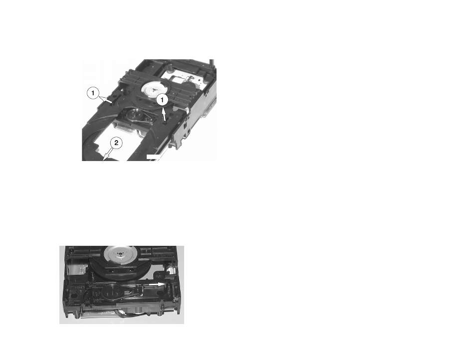
Dismantling of Tray
Service hints
1. Open the tray and release 2 catches as
shown in fig. 2
2. Pull tray out.
fig.2
Assembling of Tray
1. Check if slider is on the right side
→
see
picture below.
2. If necessary - move slider to the right end
position first.
3. Insert the Tray.
Laser Power Control & HF Amplifier (ADALAS) TZA1024/TZA1025
Pin
Name
Direction
Description
1
LD
HF-preamp
→
CD-drive
current output to laser diode
2
VCCL
+5V
laser supply voltage
3
CFIL
→
HF-preamp
external filter capacitor
4
MON
CD-drive
→
HF-preamp
laser monitor diode input
5
DIN
CD-drive
→
HF-preamp
central diode input
6
GND
GND
ground
7
PWRON
CD10
→
HF-preamp
power-on select input
8
CMFB
VrefCD10 (+3,3V / 2)
common mode feedback voltage input
9
RFFB
→
HF-preamp
external RF feedback resistor
10
RFEQO
HF-preamp
→
RF amplifier output
11
CDRW
CD10
→
HF-preamp
gain select input for CDDA/CDRW
12
EQSEL
CD10
→
HF-preamp
equalizer/speed select input
13
VCC2
+3,3V
supply voltage
14
RGADJ
GND
external laser supply gain adjust resistor
SIGNAL PROCESSOR (CD10) SAA7325
Pin
Name
Direction
Description
1
HFREF
→
CD10
comparator common mode input
2
HFIN
→
CD10
comparator signal input
3
ISLICE
CD10
→
current feedback from data slicer
4
VSSA1
GND
analog ground 1
5
VDDA1
+3,3V
analog supply voltage 1
6
IREF
CD10
→
reference current output pin
7
VRIN
CD10
→
reference voltage for servo ADC’s
8
D1
CD-drive
→
CD10
unipolar current input (central diode signal input)
9
D2
CD-drive
→
CD10
unipolar current input (central diode signal input)
10
D3
CD-drive
→
CD10
unipolar current input (central diode signal input)
11
D4
CD-drive
→
CD10
unipolar current input (central diode signal input)
12
R1
CD-drive
→
CD10
unipolar current input (satellite diode signal input)
13
R2
CD-drive
→
CD10
unipolar current input (satellite diode signal input)
14
VSSA2
GND
analog ground 2
15
CROUT
CD10
→
X-TAL
crystal/resonator output
16
CRIN
X-TAL
→
CD10
crystal/resonator input
17
VDDA2
+3,3V
analog supply voltage 2
18
LN
CD10
→
DAC left channel differential output - negative
19
LP
CD10
→
DAC left channel differential output - positive
20
VNEG
GND
DAC negative reference input
21
VPOS
+3,3V
DAC positive reference input
22
RN
CD10
→
DAC right channel differential output - negative
23
RP
CD10
→
DAC right channel differential output - positive
24
SELPLL
CD10
→
selects whether internal clock multiplier PLL is used
25
TEST1
GND
test control input 1; this pin should be tied low
26
CL16
CD10
→
NPC
16.9344 MHz system clock output
27
DATA
CD10
→
NPC
serial data output (3-state)
28
WCLK
CD10
→
NPC
word clock output (3-state)
29
SCLK
CD10
→
NPC
serial bit clock output (3-state)
30
EF
CD10
→
NPC
C2 error flag output (3-state)
31
TEST2
GND
test control input 2; this pin should be tied low
32
KILL
CD10
→
Mute control
kill output (programmable; open-drain)
33
VSSD1
GND
digital ground 2
34
V2/V3
CD10
→
NPC
versatile I/O: input versatile pin 2 or output versatile pin 3 (open-drain)
35
WCLI
NPC
→
CD10
word clock input (for data loopback to DAC)
36
SDI
NPC
→
CD10
serial data input (for data loopback to DAC)
37
SCLI
NPC
→
CD10
serial bit clock input (for data loopback to DAC)
38
RESETn
µP
→
CD10
power-on reset input (active low)
39
SDA
µP
↔
CD10
microcontroller interface data I/O line (open-drain output)
40
SCL
µP
→
CD10
microcontroller interface clock line input
41
RAB
µP
→
CD10
microcontroller interface R/W and load control line input (4-wire bus mode)
42
SILD
µP
→
CD10
microcontroller interface R/W and load control line input (4-wire bus mode)
43
STATUS
CD10
→
servo interrupt request line/decoder status register output (open-drain)
44
TEST3
GND
test control input 3; this pin should be tied low
45
RCK
→
CD10
subcode clock input
46
SUB
CD10
→
P-to-W subcode bits output (3-state)
47
SFSY
CD10
→
µP
subcode frame sync output (3-state)
48
SBSY
CD10
→
NPC
subcode block sync output (3-state)
49
CL11/4
CD10
→
11.2896 MHz or 4.2336 MHz (for microcontroller) clock output
50
VSSD2
GND
digital ground 3
51
DOBM
CD10
→
bi-phase mark output (externally buffered; 3-state)
52
VDDD1P
+3,3V
digital supply voltage 2 for periphery
53
CFLG
CD10
→
correction flag output (open-drain)
54
RA
CD10
→
servo driver
radial actuator output
55
FO
CD10
→
servo driver
focus actuator output
56
SL
CD10
→
servo driver
slide control output
57
VDDD2C
+3,3V
digital supply voltage 3 for core
58
VSSD3
GND
digital ground 4
59
MOTO1
CD10
→
servo driver
motor output 1; versatile (3-state)
60
MOTO2
CD10
→
motor output 2; versatile (3-state)
61
V4
CD10
→
HF-preamp
versatile output pin 4
62
V5
CD10
→
HF-preamp
versatile output pin 5
63
V1
innerswitch
→
CD10
versatile input pin 1
64
LDON
CD10
→
HF-preamp
laser drive on output (open-drain)
Abbreviations