Backlight signals – Planar LC640.480.33-AC User Manual
Page 11
LC640.480.33-AC Operations Manual (OM600-01)
9
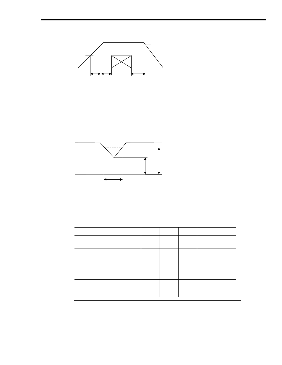
Figure 2. Power Sequencing.
data
t3
t2
t1
Vcc
4.5V
4.5V
2.7V
where: t
1
≤
10ms
0< t
2
≤
10ms
0< t
3
≤
1s
Applying video signals before V
L
is applied may cause a latchup condition. Allowing V
L
to remain “on” for a long period of time after video signals are removed—which stops
the cell scanning—may produce a latent image. In addition, there is a restriction
regarding dropouts on the V
L
supply as illustrated in Figure 3 (“Vcc”= V
L
). This is
related to the reset circuit for the LCD’s internal logic. If a dip in V
L
exceeds 10 ms in
duration or V
L
falls below 2.7 Vdc then the power sequencing procedure should be
followed.
Figure 3. V
L
Supply Dropouts.
td
Vcc
4.5V
2.7V
where:
t
d
≤
10ms
Backlight Signals
The dimming control and /DISABL inputs are analog, though the latter is intended to be
driven from either an open collector device or CMOS logic. The /ABCOFF input is a
CMOS-compatible digital input.
Table 7. Backlight Signal DC Characteristics.
Description
Min
Max
Units
Symbol
Absolute max. input voltage
-0.3
+5.3
Vdc
V
IMAX
Dimming input voltage range
0
+5.0
Vdc
V
RLUM
Recommended pot. value
10
100
K ohm
RLUM
RLUM HI source current
–
600
µA
I
RLUM
/ABCOFF input
+3.6
0
–
+5.0
+1.4
0.5
Vdc
Vdc
mA
V
IHA
V
ILA
I
ILA
/DISABL input
+4.5
0
–
+5.0
+1.0
1.3
Vdc
Vdc
mA
V
IHD
V
ILD
I
ILD
Note: Incorrect operation of the undervoltage lockout (UVLO) circuit may occur if
the /DISABL input is allowed to operate between V
ILD
and V
IHD
.