3 memory maps and description of the pld registers, Tms320c6713 memory map, Table 1: memory map of the processor – Kane Industries C6713CPU User Manual
Page 20: Chapter 3 gives an overview of the memory, To chapter 3 for further description

H
ARDWARE
R
EFERENCE
G
UIDE
MICRO
-
LINE
®
C6713CPU
Date : 28 November 2005
Doc. no. : C6713CPU_HRG
Iss./Rev : 1.1
Page : 20
3 Memory Maps and Description of the PLD Registers
3.1 TMS320C6713 Memory Map
The memory map of the TMS320C6713 is divided into several sections:
• internal
memory
• DSP
peripherals
• EMIF CE spaces CE0 .. CE3
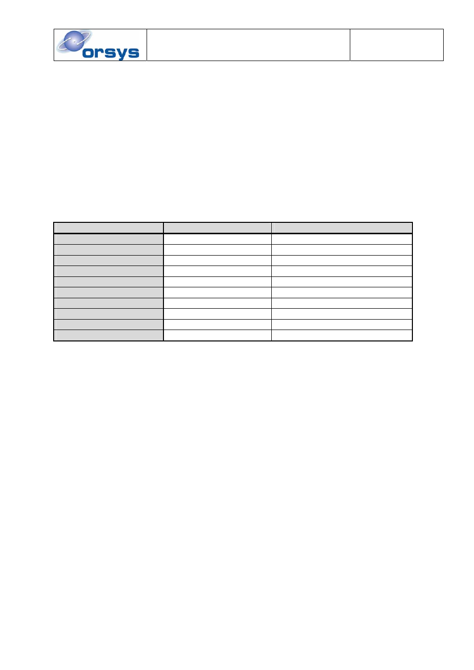
The external devices are located at different CE (Chip Enable) spaces. The EMIF bus timing of
each CE space can be individually set up. The complete memory map is shown in Table 1. For a
more detailed memory map of the DSP please refer to [4].
address range (hex)
size (bytes)
Description
0000 0000 - 0002 FFFF 192KB
Internal RAM
0003 0000 - 0003 FFFF 64KB
Internal RAM/Cache
0004 0000 - 017F FFFF 24MB - 256KB
Reserved
0180 0000 - 3C1F FFFF 938MB
DSP peripherals
3C20 0000 - 7FFF FFFF 1GB + 62MB
Reserved
8000 0000 - 8FFF FFFF 256MB (usable: 128MB ) EMIF CE0
9000 0000 - 9FFF FFFF 256MB (usable: 128MB ) EMIF CE1
A000 0000 – AFFF FFFF 256MB (usable: 128MB ) EMIF CE2
B000 0000 – BFFF FFFF 256MB (usable: 128MB ) EMIF CE3
C000 0000 – FFFF FFFF 1GB
Reserved
Table 1: Memory map of the processor
