Hardware information, Block diagram, Technical data – Spectrum Brands MI.20xx User Manual
Page 11: Block diagram technical data
Introduction
Hardware information
(c) Spectrum GmbH
11
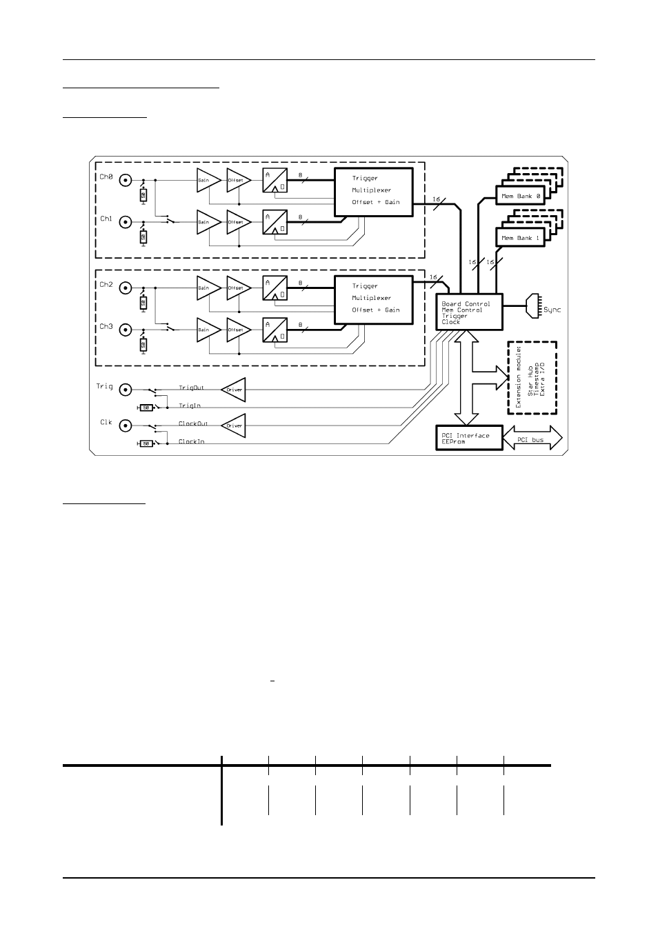
Hardware information
Block diagram
Technical Data
Resolution
8 bit
Dimension
312 mm x 107 mm
Differential linearity error (ADC)
0.5 LSB typ.
Width (Standard)
1 full size slot
Integral linearity error (ADC)
0.5 LSB typ.
Width (with star hub option)
2 full size slots
Multi: Trigger to 1st sample delay
fixed
Analogue Connector
3 mm SMB male
Multi: Recovery (re-arm) time
< 20 samples
Overvoltage protection (range < ±500 mV)
±5 V
Trigger accuracy 2/4 channel mode
1 Sample
Overvoltage protection (range > ±500 mV)
±50 V
Trigger accuracy 1 channel mode
2 Samples
Warm up time
10 minutes
Ext. clock: delay to internal clock
42 ns ± 2 ns
Operating temperature
0°C - 50°C
input signal with 50 ? termination
max 5 V rms
Storage temperature
-10°C - 70°C
Trigger output delay
1 Sample
Humidity
10% to 90%
Input impedance
50 Ohm / 1 MOhm || 25 pF
Min internal clock
1 kS/s
Power consumption 5 V @ full speed
max 3.4 A (17.0 Watt)
Min external clock
1 MS/s
Power consumption 5 V @ power down
max 1.9 A (9.5 Watt)
Trigger input:Standard TTL level
Low: -0.5 > level < 0.8 V
High: 2.0 V > level < 5.5 V
Trigger pulse must be valid > 2 clock periods.
Clock input: Standard TTL level
Low: -0.5 > level < 0.8 V
High: 2.0 V > level < 5.5 V
Rising edge is used.
Required duty cycle: 50% ± 5%
Trigger output
Standard TTL, capable of driving 50 Ohm.
Low < 0.4 V (@ 20 mA, max 64 mA)
High > 2.4 V (@ -20 mA, max -32 mA)
One positive edge after the first internal trigger
Clock output
Standard TTL, capable of driving 50 Ohm
Low < 0.4 V (@ 20 mA, max 64 mA)
High > 2.4 V (@ -20 mA, max -32 mA)
Input range
±50 mV
±100 mV
±200 mV
±500 mV
±1 V
±2 V
±5 V
Software programmable offset
±200 mV
±400 mV
±800 mV
±2 V
±4 V
±8 V
±20 V
Offset error
< 1 LSB, adjustable by user
Gain error
< 2 %
< 2 %
< 2 %
< 2 %
< 2 %
< 2 %
< 2 %
MI.202x: Noise (rms): 50 Ohm, 50 MS/s
< 0.5 LSB
< 0.5 LSB
< 0.5 LSB
< 0.5 LSB
< 0.5 LSB
< 0.5 LSB
< 0.5 LSB
MI.203x: Noise (rms): 50 Ohm, 100/200 MS/s
< 2.0 LSB
< 1.5 LSB
< 1.0 LSB
< 1.0 LSB
< 1.0 LSB
< 1.0 LSB
< 1.0 LSB
Crosstalk 5 MHz signal, ±50 mV input, 50 Ohm
< 62 dB